 |
| |||||||||||||||||||||||||||||||||||||||||||||||||||||||||||||||||||||||||||||||||||||||||||||||||||||||||||||||||||||||||||||||||||||||||||||||||||||||||||||||||||||||||||||||||||||||||||||||||||||||||||||||||||||||||||||||||||||||||||||||||||||||||||||||||||||||||||||||||||||||||||||||||||||||||||||||||||||||||||||||||||||||||||||||||||||||||||||||||||||||||||||||||||||||||||||||||||||||||||||||||||||||||||||||||||||||||||||||||||||||||||||||||||||||||||||||||||||||||||||||||||||||||||||||||||||||||||||||||||||||||||||||||||||||||||||||||||||||||||||||||||||||||||||||||||||||||||||||||||||||||||||||||||||||||||||||||||||||||||||||||||||||||||||||||||||||||||||||||||||||||||||||||||||||||||||||||||||||||||||||||||||||||||||||||||||||||||||||||||||||||||||||||||||||||
|
| ||||||||||||||||||||||||||||||||||||||||||||||||||||||||||||||||||||||||||||||||||||||||||||||||||||||||||||||||||||||||||||||||||||||||||||||||||||||||||||||||||||||||||||||||||||||
E. Vogel
Feedback - Tanzania
91-34-0306/6
CRYSTAL
Lehr- und Lernmittel,
Informationen, Beratung
Educational Aids,
Literature, Consulting
Moyens didactiques,
Informations, Service-conseil
Material did�ctico,
Informaciones, Asesor�a
Deutsche Gesellschaft f�r Technische Zusammenarbeit (GTZ) GmbH
A script for students at
TANZANIAN TECHNICAL SECONDARY
SCHOOLS
written 1986-1989 at Moshi Technical Secondary School
|
by: |
J. Nyanza |
Moshi Technical Secondary School POB 3814/MOSHI/TANZANIA |
| |
E. Vogel |
Br�derstr. 42/13595 Berlin/Germany |
retyped 1993

Figure
|
| ||||||||||||||||||||||||||||||||||||||||||
Radio and Electronics (DED Philippinen, 66 p.)
1. INTRODUCTION
AN INTRODUCTION WHAT FOR?
At first: because the field of electronics is growing very fast. Therefore it is not possible to give an always fitting definition of what ELECTRONICS is.
Secondly: the importance of this field is probably becoming very high - in Tanzania too. So it is necessary to have at least a rough idea of what one is dealing with, if one is studying ELECTRONICS.
1.1. A TRIAL TO STATE A DEFINITION OF ELECTRONICS
In older books you find as an explanation for the term Electronics: Electronics are electric devices in which in some components the electrons are flowing in gases. Components which let the electrons flow in gases, are VALVES.
But even if you have only a very vage idea of the components found nowadays in radios, you know very well, that there are rarely used valves.
Additional you might know too, that radios are only one example of an electronic device.
In all those electronic devices nowadays there are used transistors instead of valves. Transistors are so-called SEMICONDUCTING components. But if all electric devices including semiconducting components would be called electronic devices, the term would be no more helpful.
Because almost each electric device includes this type of components now. During the last decades more and more electric circuits have been invented which had mainly the purpose to control another electric circuit.
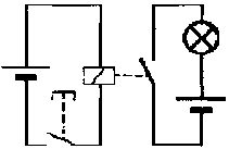
fig. 1
To give an example: In a so-called voltage-stabilizer you will find a circuit which would measure the voltage at the input of the stabilizer, and the circuit of the equipment which needs the stabilized voltage. The second circuit will be controlled by the first one, in order to keep the voltage at the sensitive equipment stabile. Controlling in this connection can most simply be: to switch off and on, the lamp, or to dim it. This controlling was done at first by relays or by motoroperated rheostats. The relays and the motor driven rheostats are so-called ELECTROMECHANIC components. In such a component there are always moving parts, and this fact has two main disadvantages:
1. the speed of reaction of these components is rather low (a relays for example is only able to switch off and on 100 times/second)2. the moving parts are worn out very fast, therefore the service life of those components is rather limited. (relays can be operated only about 1 million times). So it was very important to search for means of controls which do not have those disadvantages.
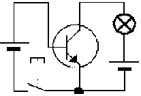
fig. 2
When the development of radios started it was depending on the development of components like valves, transistors and thyristors. With those new components it was possible now to control circuits:
1. directly without a mechanic interface, and2. with much higher speed (several million times per second).
So let us agree on the following definition for this script here: CIRCUITS WITHOUT MECHANICAL SWITCHES WHICH ARE DESIGNED TO CONTROL OTHER CIRCUIT SWITH A VERY HIGH SPEED OF REACTION ARE CALLED ELECTRONIC CIRCUITS
1.2. A SHORT HISTORY OF ELECTRONICS
Although Electronics started just about eighty years ago. It went through quite some stages within this rather short period. It started in the 20ties of this century, when RADIO TECHNOLOGY was born.
The first challenge was to produce more sound for the listener, and this made it necessary to invent VALVES.
During the 30 ties there was the challenge to handle higher frequencies, and when this goal was achieved, it was possible to think of trials with RADAR and TELEVISION.
In the 40ties the first experiments with so called “ELECTRONIC BRAINS” (later they were called COMPUTERS) were carried out. At the end of the 40ties - just after the second world war - the SEMICONDUCTORS were more closely researched and led to the inventing of DIODES and TRANSISTORS.
Those new components were very helpful in building much smaller computers which were very important for the first travels to space.
Now the field of application of electronic equipment grew very fast.
On other very important step connected with this field of technology was the change of method to manufacture the circuits:
- while in the first radios the circuit had been WIRED like all the devices- lateron it was found more economical (because it was much faster and possible with much less faults) to wire it by so called PRINTED CIRCUITS (Insulating boards with copper lines on it, which represent the wires, and which can be “printed” on the boards)
- the next step was to find a way to “engrave” whole circuits on a very small piece of semiconducting material. Such circuits were called then “INTEGRATED CIRCUITS” - they can hold nowadays thousands of transistors.
1.3. CLASSIFICATION OF ELECTRONIC DEVICES
Basically there are no borders between all fields of electronic devices, as there are:
- communicationsystems (radios, transmitters, recorders etc.)- data processing systems (computers and measuring instruments)
- controlsystems (in machines, aeroplanes powerstations)
In all those applications the same technical principles and similar basic circuits are applied.
Nevertheless, if one has a general look at all these different kinds of circuits, he will find two different FAMILIES of circuits differentiated according to the method of translating the original physical effect (for example the air pressure of the sound) into an electric signal.
The first family is the so called “ANALOGUE CIRCUIT”. Here the shape of the output-signal is equal to the input-signal.
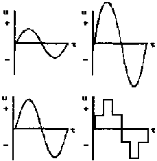
fig. 3
The second family is the so-called “DIGITAL CIRCUIT”. Here the shape of the outputsignal represents the input signal in form of digits(steps). These years the development of electrical technology is very fast. Therefore in future you might easily find circuits of one or the other family which you would have not expected in a special device of a that certain kind.
|
| |||||||||||||||||||||||||||||||||||
Radio and Electronics (DED Philippinen, 66 p.)
2. PRINCIPLES OF RADIO COMMUNICATION UNICATION
2.1. BASICAL IDEAS ABOUT COMMUNICATION
The basical idea of the term COMMUNICATION is: to transfer an idea (a SIGNAL) from one from one brain of a human being (a SIGNAL-SOURCE) to the brain of another human being (a RECEIVER).
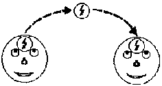
fig. 4
The “normal” way of communication is of course to speak with each other. But which “TECHNOLOGY” is used during speaking? Obviously, the idea is translated into words.
The words are produced in terms of voice (or SOUND). This sound in physical sense of the word is nothing else than a special sequence of airpressures. These airpressures will cause vibrations everywhere.
They will hit the inner ear of the “receiver” and will be retranslated in his brain into the original idea. This normal way of communication is no more possible if the distance between the “signalsource” and the “receiver” will make it impossible to understand each other anymore. While the past human beings found different possibilities to overcome this problem.
2.2. DEVELOPMENT OF LONG DISTANCE COMMUNICATION

fig. 5a
There are two people who want to communicate with each other but the distance is too far... WHAT CAN BE DONE?

fig. 5b
A very old fashioned way to solve this problem was to send a MESSENGER.

fig. 5c
Since about 100 years there is a more convenient method of communication: the TELEPHONE.

fig. 5d
Since about 50 years there is another - even more convenient method of communication the RADIO TECHNOLOGY.
SUMMING UP:
Since the PROPAGATION of SOUND is very limited in distance for communication across longer distances another means of transporting the SIGNAL is necessary.
As we are reminded to by the sketches above, COMMUNICATION SYSTEMS have been developed step by step through the last century.
All those different technologies are working in between the two ends of the original way of communicating.
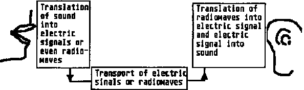
fig. 6
Even the most modern communicationsystem is working on the same overall system:
FIRST: there has to be a method to translate sound (air vibrations) into an ELECTRIC OSCILLATIONS (current or voltage oscillations).SECOND: there has to be a method to transport this electric signal across huge distances Either by wires or by so called ELECTROMAGNETIC WAVES (also called RADIOWAVES)
2.3. FIDELITY AND DISTORTION
We agreed already: the AIM OF COMMUNICATION is to transport the IDEA (the SIGNAL) totally correctly from the ORIGIN (the TRANSMITTER) to the ADDRESS (the RECEIVER).
But it is easy to imagine, that even in the original way of communication (speaking with each other) very often the idea was not received properly.
As the possibilities of arising faults are increasing with increasing complexity of the system in use, it is easy to understand, that radio technology is mainly a struggle to get a good or at least a satisfying RECEPTION.
The quality of the equivalence of the signal at the start of the communication (INPUT fig. 7a) and the signal at the end of the communicationline (OUTPUT fig 7b or 7c) is called FIDELITY.

fig. 7a
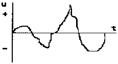
fig. 7b
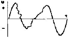
fig. 7c
The rate of difference between INPUT and OUTPUT is called DISTORTION.
|
| ||||||||||||||||||||||||||||||||||||||||||||||||||||||||
Radio and Electronics (DED Philippinen, 66 p.)
3. TRANSDUCERS
As we said already: at the beginning of each modern communicationsystem the sound has to be converted into an electric signal and at the end again the electric signal has to be translated back into sound. This task is carried out by devices which are called in general TRANSDUCERS.
Whereby the transducers which translate sound into an electric signal are called MICROPHONES and those which translate an electric signal back to sound are called EARPHONES or LOUDSPEAKERS.
Until today there was not found a way of translating sound directly into an electric signal it must be always gone the roundabout via mechanical forces.
Hold a piece of paper sensitively in your hand, position it directly in front of your mouth and start talking loudly against the paper. You will experience, that the paper is moved (vibrated) to an for by the sound. Result: sound can move by light pieces of material which show a big area vertically to the direction of the movement of soundwaves. Sound waves are exerting forces on to these light and flat pieces which we will call from now on a DIAPHRAGM. On the other hand the leather on top of a drum is another type of diaphragm. This diaphragm is able to produce sound if it is moved to and for (if it is oscillating). These considerations make it very clear, why we will find at the beginning and at the end of our communication system always a diaphragm, as shown in fig. 8.
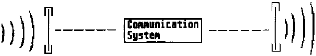
fig.
8
3.1. MICROPHONES
CARBON MICROPHON is a very old type but still in use when a cheap microphon is desired and fidelity is not so important. CARBON GRANULATES change their resistance, if they are pressed together by an external force. The inner hollow part of the microphon is filled with this type of carbon particles. At the front of the microphon is fixed a very thin sheet of metal which is here the diaphragm, and at the backside is fixed a second metalplate which stands here as an electrode to give contact to the carbon granulates.
When exposed to sound the diaphragm is moved by the air oscillations, and the pressure on the carbon granulates changes according to the frequency of the air-oscillations. Therefore the overall resistance of the carbon granulates changes according to the frequency of the sound.
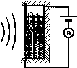
fig. 9
ELECTROSTATIC MICROPHON
Is working like a variable capacitor. The diaphragm is made from metal and stands for one plate of the capacitor. It is positioned very near to a second metalsheet with a lot of holes in it a few tens of millimeter inside of the microphone. This second metalplate stands for the second plate of the capacitor. If the diaphragm is hit by soundwaves it moves to and for, and by doing so, the distance between the tow plates changes. As well know from physics, the change of the distances lets also change the capacity of the capacitor. So the whole microphone stands for a capacitor which changes its capacity according to the sound waves hitting the diaphragm.
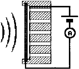
fig. 10
ELECTRODYNAMIC MICROPHON
Here a coil is fixed to a diaphragm made from insulating material (like cardboard):
This coil is positioned free within the gaps of a strong permanent magnet.
If the diaphragm is moved by soundwaves, the coil is moving to and for as well.
This movement causes induction of a voltage in the coil and so this microphon is producing a voltage depending on the frequency of the sound waves.
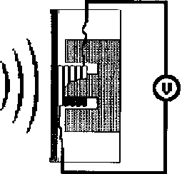
fig. 11
CRYSTAL MICROPHON
Here is used the so-called PIEZO EFFECT. If a crystal is exerted to pressure there will appear a voltage across its edges. The force to press is produced again by diaphragms, now positioned in front and behind the crystal. If the diaphragms are moved to and for by air-pressures the microphone generates a low voltage which has the same frequency as the sound wave have it.
fig.
12
3.2. LOUDSPEAKERS
ELECTRODYNAMIC PRINCIPLE
Actually this type is working just the opposite way of the electrodynamic microphone. A coil fixed to a diaphragm is suspended within the field of a permanent magnet. If a changing current is passed through the coil, there will arise a force which will tend to move the coil to and for. As the diaphragm is connected to the coil it will be moved to and for according to the frequency of the current, and by doing so it will produce sound of this frequency. Most of the earphones and loudspeakers used nowadays work on this principle.
fig. 13
ELECTROSTATIC PRINCIPLE electric charges exert forces on each other.
If one plate of a capacitor is fixed on the housing of the loudspeaker and the other plate is fixed to the diaphragm, the diaphragm can be moved, by the forces of the electric charges brought on the plates by an ac-current. This kind of loudspeaker is found very rarely.
fig. 14
PIEZO ELECTRIC PRINCIPLE
Special crystals are not only able to produce voltage if they are under pressure, but they are able to produce forces if there is a voltage connected to their edges.
This principle is not very common up to now in connection with radios, but it is more and more used to produce special sounds for example in computers.

fig.
15
3.3. THE TELEPHON SYSTEM
With the devices explained during the last chapter, you are able now to understand how a normal telephon circuit connected by wires is functioning. Just imagine in the circuit shown above is used a mocrophon of the CARBON TYPE and an earphone working on the electrodynamic principle.
fig.
16
3.4. PROBLEM OF FREQUENCY RANGES
You can imagine for sure, that a railway engine for example cannot “oscillate” (to move to and for) ten times a second, while a leaf of a tree can do that easily. The difference between both is obviously their mass. This consideration shows: mechanical devices are very limited in the range of oscillations they can follow. This problem forces the designer of a communicationsystem first to find out what range of oscillations will be required within that system. From now on we will call the oscillations FREQUENCIES and the range required will be called the FREQUENCY SPECTRUM. During the last chapter we have been talking about the translation of sound into electric signals. When we are deciding which material should be used for the diaphragm. It is obviously very important to know the highest and the lowest frequency of sound. This frequency range is called SPECTRUM OF AUDIO FREQUENCIES. If we connect a loudspeaker to a Low-frequency-generator and if we listen to the sound produced by the speaker we will find, that we start to hear sound at a minimum frequency of about 50 Hz and most of us will not hear any sound anymore, if the frequency reaches values above 18 kHz. Therefore the audio frequency spectrum is defined as the range between 50 and 20 kHz.
3.5. BANDWIDTH
As we already could see during the experiment described above, we can produce a much wider range of frequencies than the range we can listen to. Our ears are able to receive soundwaves within special limits, the range of audible (hearable) waves is called also a BANDWIDTH. We can say our ears have a bandwidth of 50 to 20000 Hz. We will come across these terms several times while dealing with radiotechnology.
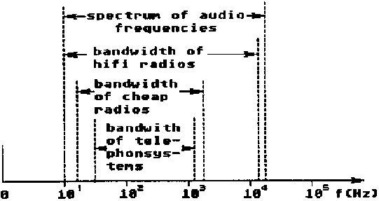
fig. 17
The graph shown in fig 17. explains again what a bandwidth is, and it shows too how different the bandwidths are for different sophisticated communicationsystems. Keep in mind: Even though the bandwidth of a telephon system is very narrow in comparison with bandwidth of the audio frequencies we are able to understand the partner at the other end of the communication line.
CHECK YOURSELF:
1. What is the meaning of the term COMMUNICATION actually?2. What is the difference between a telephon and a radio system?
3. How are the devices called which are translating sound waves into electric signals?
4. How are the four different types of microphones functioning?
5. Which different types of loudspeakers do You know?
6. What is the meaning of the terms “fidelity” and “distortion”?
7. What is the meaning of the terms “Spectrum” and “bandwidth”?
8. Applying your knowledge of Ohms Law try to describe how the circuit shown in fig. 16 manages to produce the
|
| |||||||||||||||||||||||||||||||||||||||||||||||||
Radio and Electronics (DED Philippinen, 66 p.)
4. RADIOWAVES
While with telephonsystems the medium of “transport” for the signal was an electric current on a wire, you know that radios don't get their signal by a wire. The medium used here are the so called ELECTROMAGNETIC WAVES and from the huge overall range of electromagnetic waves (10-1015Hz) the SPECTRUM called the RADIOWAVES uses (105-1010Hz).
Before we can go on to talk about the devices of transmitting and receving these radiowaves, we have to know the basics of them.
4.1. ORIGIN OF RADIOWAVES
You know that, whenever there is a voltage between two points, an electric field is arising between these two points. You also learnt in Basic Electrical Science that whenever a capacitor is charged, one plate will be positiv and the other negativ. The consequence of these two facts is, that an electrical field, having a direction towards the positivly-charged plate, is build up between the capacitor plates as shown in figure 18 below.
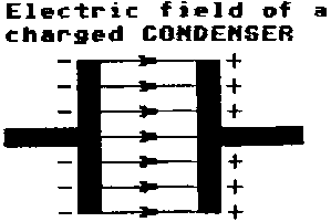
fig. 18
In the same way, the voltage difference between the two wires of an aerial also generates an electric field, which has a pattern and direction that you can see in fig. 19.
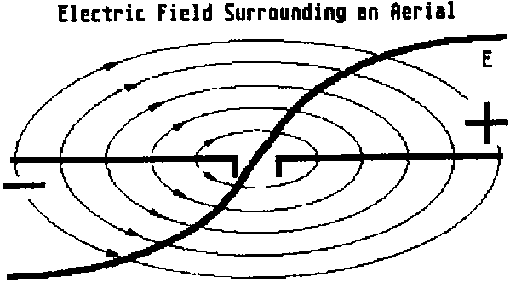
fig. 19
Besides this electric field, there is also a magnetic field, which is generated by the aerial current. The plane of this magnetic field is at right angels to the direction of the current flow; and therefore is at right angles to the aerial (see below), the electrical and the magnetic fields are therefor at right angles to each other.
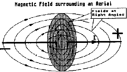
fig. 20
These electrical and magnetic fields alternate about the aerial-building up, reaching a peak, collapsing and building up again in the opposite direction at the same frequency as the aerial current.
In the process of building up and collapsing, a portion of these fields escape from the aerial, and become the electromagnetic waves which radiate through space, conveying the transmitted intelligence to distant receivers.
4.2. PARAMETERS OF ELECTROMAGNETIC WAVES
Electromagnetic waves travel with a VELOCITY of 300 000 km/sec. The FREQUENCY of radiowaves (oscillations per second) can be between 100 000 Hz and 300 000 000 Hz (100 kHz to 300 MHz). KEEP IN MIND there is a MINIMUM FREQUENCY of at least 30 kHz, only oscillations above this minimum are propagated. The AMPLITUDE is the maximum amount of electric field or magnetic field reached per one cycle. Electromagnetic waves have obviously two components the electric and the magnetic part, both are positioned at 90° to each other. After leaving the aerial the direction of both components is not changed, this means, we will receive the same waves under the same direction as they are transmitted. The way how the waves are produced (concering the direction of the components) is called their POLARISATION! Knowing this fact, we can easily understand why the reception can be improved by the direction of the aerial.
4.3. PROPAGATION OF RADIOWAVES
You know that the function of an aerial is to radiate electro-magnetic energy into space. Once this energy is released from the aerial, it will travel through space until it is picked up by the receiving aerial or until it stikes an object and is reflected off it, as it is the case with radar transmissions. It is therefore important for you to know what happens to a radiated wave in space
- what its path is,
- if it is absorbed by the earth,
- if it is reflected by the sky and so on.
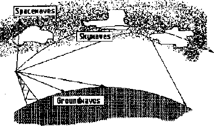
fig. 21
In order that you will be able to tell how far the wave will travel before it can be picked up. The subject of what happens to a radiated electro-magnetic wave once it leaves the aerial is called the theory of WAVE PROPAGATION. When a radiated wave leaves the aerial, part of its energy travels along the earth, following the curvature of the earth. This is called the GROUND WAVE. Other waves which strike the ground between the transmitter and the horizon are called SPACE WAVES; and those which leave the aerial at an angle bigger than that between the aerial and the horizon are called SKY WAVES. The ground wave, the space waves and the sky waves all cary the transmitted intelligence.
But at certain frequencies one of the wave-types will be much more effective in transmitting the intelligence than will the others.
At comparatively low frequencies, most of the radiated energy is in the ground wave. Since the earth is a poor conductor, the ground wave is rapidly reduced, or “attenuated”, by absortion and is therefore not effective for transmissions over great distances unless large amounts of transmitted power are used.
The medium and long wave-band broadcast frequencies are examples of transmissions using ground waves. At these frequencies the effective radiating area usually lies within 200 miles radius from the transmitter. Stations more than 400 miles away from each other can therefore transmit on the same low frequencies, and yet not interfere with each other.
SKY WAVES AND GROUND WAVES
At first sight, one would think, that sky waves can serve no useful purposes, since they will only travel straight out into space and get lost.
For very high frequencies, this actually happens, and the skywaves is useless. But below a certain critical frequency the skywave does not travel into space: it is bent back to earth in the upper layers of the atmosphere.
This returning wave is not sharply reflected, as is light from a mirror. It is bent back slowly, as if it were going round a curve: it is therefore called a refracted wave.
This refracted wave, once it returns to earth, is reflected back into the sky again where it is once again refracted back to earth. This process of refraction from the sky and reflection from the earth continues until the wave is completely attenuated - the energy of the radiated wave dropping as its distance from the transmitting areal increases. A receiving aerial will be able to pick up a signal at any point where the refracted wave hits the earth. If the sky wave were radiated to the sky at one angle only, of course, no signal would arrive at any points save. Sky waves, however are radiated from the transmitter at many angles, there are therefore large areas of the earth's surface at which reception of signals form a particular transmitter as possible.
As the angle of radiation of the sky wave gets steeper, a point is eventually reached at which the wave is not longer refracted back to earth, but continues travelling into space. As a result, there is a zone around the aerial in which no refracted sky wave hits the earth.
Since the ground wave itself is only effective over a short distance, there exists a zone between the maximum effective radiating distance of the ground wave and the point where the first sky wave is refracted back to earth, which is an aerea of RADIO SILENCE in which no signals from this particular transmitter are received. This zone is called the SKIP DISTANCE.
The critical frequency, which is the frequency above which no sky wave (whatever its angle of radiation) can return to earth, varies - depending on numerous factors such as the time of day, the time of year, the weather, and others.
THE SPACE WAVE
At frequencies above the critical frequency, neither the ground wave nor the sky wave can be used for transmission. At these high frequencies, the ground wave is rapidly attenuated, and the sky wave is not refracted back to earth.
The only radiated wave which can be used for transmission at these frequencies is one that travels in a direct line from the transmitting aerial to the receiving aerial.
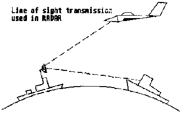
fig. 23
This type of transmission is called LINE-OF-SIGHT TRANSMISSION; and the radiated wave is called a SPACE WAVE.
Line-of-sight transmission is used in RADAR for detecting enemy aircraft, and in ship-to-plane communication. The frequencies used are usually above 3b megacycles.
FADING
Sometimes a receiving aerial picks up two signals which have travelled along different paths but originated from the same transmitting aerial. One signal will travel direct from the aerial; the other may have been reflected to the receiver off, say, an aeroplane.
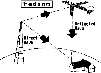
fig. 24
Since the relative length of the paths of these signals is constantly changing, the two signals will sometimes be in phase, and at other times out of phase - thus tending either to cancel or to reinforce one another. The result is a variation in signal strength at the receiver end which is called FADING.
4.4. SPECTRUM OF RADIOWAVES AND BANDS OF RADIOWAVES
There follows now an outline of the components of a radiated wave which are used for transmission at various frequencies:
From 30 to 300 kilocycles (low frequency band), the ground wave is largely used for medium-range communication, since it its stability is not affected by seasonal of weather changes. For very long distance communication, the sky wave is used.
From 300 to 3000 kilocycles (medium frequency band) the range of the ground wave varies from to 15 to 400 miles. Sky wave transmission is excellent at night for ranges up to 8000 miles. In daytime however, sky wave transmission becomes erratic, especially at the high end of the band. From 3 to 30 megacycles (high frequency band), the range of the ground wave decreases rapidly, and sky wave transmission is highly erratic on account of the seasonal factors previously mentioned. Space wave transmission begins to become important.
From 30 to 300 megacycles (very high frequency band - or VHP), neither the ground wave nor the sky wave are usable, and space wave (line-of sight) transmission finds major application.
From 300 to 3000 megacycles (ultra-high-frequency band - UHF), space wave transmission is used exclusively.

fig.
25
|
| |||||||||||||||||||||||||||||||||||||||||||||||||
Radio and Electronics (DED Philippinen, 66 p.)
5. MODULATION OF RADIOWAVES
Let us first sum up, what we know till here:
1. Our ears are able to receive frequencies within the so called audio-frequency spectrum which starts at about 30 Hz and ends below 20 000 Hz.2. Only frequencies of a minimum of about 30 000 Hz can be transmitted in form of electromagnetic waves.
3. Therefore it is easy to understand that we will hear nothing if a radio receiver is picking up a very strong transmission of a certain radiostation unless....
4. ... there is an audio signal transmitted as well.
HOW TO TRANSMIT THEN THE WANTED AUDIOSIGNAL BY MEANS OF RADIOWAVES?
The technical solution for this problem is: to let the radio frequency signal “carry” the audiosignal.
The process of charging the “lorry” (putting the audiosignal on the carrierwave) is called MODULATION.
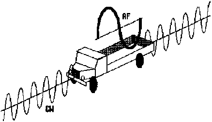
fig. 26
Modulation means actually “varying”. So modulation of the carrierwave means to change the carrier-wave in one of its aspects, proportionally to the amplitude of the audiosignal.
The carrierwave has two main characteristics which determine its shape: the FREQUENCY and the AMPLITUDE.
To ENCODE a message (here to encode the audiosignal on the carrierwave) it is enough to change one of these two factors. Considering this fact, it is easy to understand why there are two methods of modulation.
5.1. THE AMPLITUDE MODULATION (AM)
As the term tells us already, here the amplitude is varied. How this is done shows fig. 27:

fig. 27
As long as the audiosignal has an amplitude of “0”, the carrierwave has its original amplitude.
As soon as the audiosignal starts to have a positive amount, the amplitude of the carrierwave will rise proportionally to the amount of the audiosignal and therefore it will have an amplitude bigger than the original carrier amplitude.
As soon as the audiosignal starts to be negatively directed, the amplitude of the carrierwave will be diminished. But keep in mind: the carrierwave may never reach an amplitude which is “0”.
The INTENSITY OF THE MODULATION can vary from case to case.
It is called the PERCENTAGE OF MODULATION?

5.2. FREQUENCY MODULATION (FM)
Here the term itself shows already how it is achieved: The carrierwave in this case has an always constant amplitude. If there is no audiosignal there will be broadcasted exactly the basical carrierfrequency CF (for example 10 MHz.).
As soon as there is an AF-signal coming in, this carrierfrequency will be varied.
If there is coming in a positive halfwave of the audiofrequency the carrierfrequency will be increased. This rise can reach a maximum of 75 kHz in case of the highest permitted amplitude of the AF-signal. This means the outgoing signal will be 10.075 MHz in case of a maximum positive amplitude.
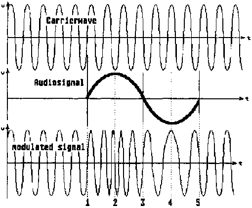
fig. 28
If there is a negative halfwave coming in, the carrierfrequency will be diminished.. As soon as the audiosignal has reached again “0” the outgoing signal has exactly the original frequencao of 10 MHz.
5.3. SIDEBANDS
Both types of modulations have the effect, that there is special spectrum of frequency leaving the aerial. Beside the actual carrier-wave there are higher and lower frequencies. They are called the SIDEBANDS. The frequencies higher than the carrier-frequency are called UPPER SIDEBANDS the frequencies lower than the carrierfrequency

fig.
29
5.4. TRANSMISSION OF RADIOSIGNALS
As we don't have to learn about the circuits for a radio transmitter within this course, we will only describe roughly how it works. For such a rough introductory description it is helpful to use a special kind of diagram. This diagram is called a BLOCKDIAGRAM, and it shows only rectangular blocks, which visualize circuits generally, by announcing their function only.

fig. 31
Fig. 31 shows the blockdiagram of a radio transmitter and fig 32 shows the signal how it will look like when it leaves the aerial.

fig. 32
This course will deal from now on, mainly with the following question:
HOW TO RECEIVE THIS SIGNAL IN A RADIO-RECEIVER?
HOW TO PROCESS THIS SIGNAL UNTIL IT CAN BE HEARD AT THE SPEAKER?
CHECK YOURSELF:
1. Explain how electromagnetic waves are produced!2. Mention the parameters of electromagnetic waves!
3. Which different waves do you know and which are their special characteristics?
4. Which different bands of radiowaves do you know?
5. Which of these bands is useful for long distance communication?
6. Which of these bands is useful for short distance communication?
7. Give the frequency ranges of the different wavebands?
8. What does the term Fading meand, and what is its effect on reception?
9. Which band is used for communication from spaceships to earth and back?
10. What is the reason why long distance radio communication is not totally reliable?
11. What does the term modulation mean?
12. Which types of modulation do you know?
13. Calculate the “% modulation” for the shown case in fig. 30!
|
| |||||||||||||||||||||||||||||||||||||||||||||||||||||||||||||||||||||||||||||
Radio and Electronics (DED Philippinen, 66 p.)
6. RECEPTION OF RADIOSIGNALS (AM - TYPE)
6.1. AERIAL
The origin of any signal processed in a radio receiver is the signal picked up by the aerial.
So the radiowave is an electromagnetic wave the reception (picking up) can be achieved generally in two different ways.
RECEPTION OF THE MAGNETIC PART OF THE RADIOWAVE:
This can be achieved by a so called FERRIT ROD AERIAL. Such an aerial consists of a ferrite rod around which the one or more coils of copperwire are wound. The advantage of this type of aerial is, that it needs only little space and therefore it can be built inside the cabinet of even rather small radios.
But keep in mind: the bigger the ferritrod is, the more powerful is the received signal.
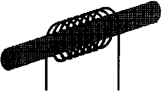
fig. 33
The reception of this aerial is depending very much on its position in relation to the received signal. It is receiving best, if the rod is hit perpendicular by the waves. This fact explains, why a receiver with that kind of aerial can have very different output power at the same spot, if the receiver is turned into another direction.
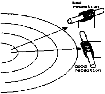
fig. 34
RECEIVING THE ELECTRICAL PART OF THE RADIOWAVE:
This can be achieved by aerials of different construction.
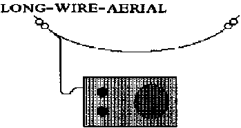
fig. 35
If the radio is stationary we can improve the reception by a long piece of or just a so called TELESCOP-AERIAL (as you find with most of the small portable radios). In generally one can say: as longer the aerial as better its reception.
DIPOL-AERIAL
While the aerials shown above are mostly used for long- and medium-wavebands, we have to use another type for higher frequencies.
The so called dipol-aerial consists of: either two wires constructed as fig. 36a shows (an OPEN DIPOL) or a loop of a wire constructed as fig. 36b shows (a FOLDED DIPOL).
Both types work best, if they have a length of about one half of the waves which are intended to be received. But even though we talk in such a case of ADJUSTED or TUNED aerials, this does not mean, that this aerial is only able to receive one single radiostation. All aerials are able to receive a rather wide range of frequencies with reasonable results.
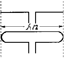
fig. 36
This is on the one hand a big advantage (we don't need a special aerial for each different radio station we want to receive). On the other hand it causes problems for the radio technician, because we will always find at the terminals of the aerial a lot of different incoming signals, which are mixed together.
The above stated fact makes already clear what has to be done first with the signals found at the terminals of the aerial: we cannot just amplify the signal coming from the aerial, because under this condition we would hear an awful mixture of sounds of all the radioprograms transmitted in the surrounding of the radio.
We have to make sure first, that only the signal of the desired station will be processed during the next stages of our radio receiver.
This process of barring the other stations out and letting through only one station is called FILTERING. In which block the filtering is achieved, will be explained in the next chapter.
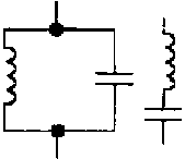
6.2. THE TUNED CIRCUIT
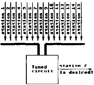
fig. 37
The signal at the terminals of the aerial consists of a mixture of signals of all the surrounding radio stations as shown in fig. 37.
But we want to listen only to one of those stations.
How to sort out one single station?
All of them carry audiosignals, - but this fact does not help us here... (Audiosignals are all of the same frequency spectrum). On the other hand all of them have a carrierfrequency as well. And those carrierfrequencies are - for sure different from each other (otherwise the radiostations would be operated against the law). So we can sort the desired program out, by letting through to the next stages of our receiver only the radiosignal with the carrierfrequency of our desired radio station.
The circuit which will be able to do this filtering is the so called TUNED CIRCUIT and it consists of at least one capacitor and an inductor. How the filtering is achieved really, we will discuss in details later in chapter 6., at this stage of explanation it is just important to keep in mind, that we will find in each radio at least one of those tuned circuits connected right to the terminals of the aerial.
6.3. INCIDENTAL REMARK ON BLOCK DIAGRAMS
Electronic devices consist nowadays in most cases of a lot of different circuits, each of it having a special purpose playing a special role in the “oncert” of the whole device. Each of the circuits itself can be very complicated.
To visualize the function of such devices, it would be far too confusing if we would draw all the components and interconnections in those different circuits at once.
Therefore nowadays more and more another method of visualization is used: the so-called BLOCK DIAGRAMM.
Here each different circuit playing a special role is symbolized by only a “block” (a rectangle carrying a special symbol or a word explaining the function). The blocks are interconnected by lines which show the flow of the signals or of energy from one block to the other.
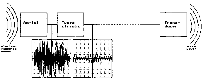
fig. 38
Using this method of visualization we can draw at this stage of explanation a block diagram of the parts of a radio which we have come to know already.
Fig. 38 shows what we can draw up to now. Additional to the normal blockdiagramm, we find in this drawing the type of signal, appearing between those blocks.
If you have a closer look to the output signal of the tuned circuit you will find, that it is exactly the signal which would leave the transmitter of the radiostation we want to listen to.
But you should know: this drawing showing an ideal situation Normally you will have a huge attenuation on the way from the radiostation to the receiver, and the signal leaving the tuned circuit is very small (often less than a milli Volt).
If we receive the signal of a radiostation very near by (let us say a few hundred meters) this signal would be - with some luck - a few hundred milli Volts.
A sensitive earphone can produce sound with such a low voltage, but KEEP IN MIND: EVEN IF THE OUTPUT SIGNAL OF THE TUNED CIRCUIT IS POWERFUL ENOUGH YOU CANNOT LISTEN TO IT BY CONNECTING AN EARPHONE DIRECTLY.
6.4. DETECTOR OR DEMODULATOR
The reason for the effect stated at the end of the last chapter, can be explained very easily, if we have a closer look to the signal produced by the tuned circuit: This signal is actually a “mixture of two signals” - the carrierfrequency modulated by the audiofrequency.
- The earphone - when connected to the terminals of the tuned circuit - will be passed by a current with a frequency which is the carrierfrequency. If the diaphragm would be able to follow this carrierfrequency it would produce “air pressure oscillations” of a frequency far above the range of audiofrequencies, therefore we would not hear anything.
So the diaphragm cannot follow these high frequencies, it will be at rest. Therefore we cannot hear anything at all.
CONSEQUENCE:
In order to be able to listen to anything, we have to “remove” the carrierfrequency from the modulated radiosignal (to discharge the audio signal).
The process of removing the carrierwave is called DEMODULATION and it is carried out by a circuit called DEMODULATOR or DETECTOR.
If we assemble the blocks which we came to know up to hear, we would be able to hear at least a strong radiostation which is near to our receiver.
Fig. 39 shows the system which can be achieved if we do so. By doing so we have got a very simple kind of radioreceiver called a CRYSTAL RADIO.
This was the type of radio which was used first during the first days of radio-technology.
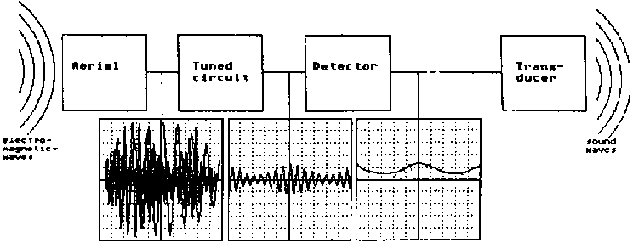
fig. 39
But you can very easily imagine, why this kind of radio was not a satisfying one: The sound produced was very weak and only one person could hear something if he was lucky enough to receive a station which could deliver enough energy for his earphones.
How could this “receiver” be improved? Of course have you have heard something about the law of CONSERVATION OF ENERGY.
If you apply this law on our crystal receiver, you will find out very easily, that the transducer (the earphone) can only produce sound energy with a maximum which is limitted by the input energy of the aerial.
This means as well: If we want to increase the sound energy we have to add energy to the energy from the aerial. This energy must be supplied within our radio by a so called poer supply.
6.5. POWER SUPPLY
This part of the radio has to deliver a certain amount of a rather constant dc-voltage.
But this power supply alone will not helps us, because we cannot connect it directly to the transducer for example. If we would do so, we would hear only one crack and nothing else, because the current flowing through the coil of the earphone or loudspeaker would be constant and therefore the diaphragm would be at rest afterwards (not producing any sound).
This means: the current flowing from the power supply to the transducer has to be controlled in a way that the diaphragm of the transducer will oscillate with the frequency of the AF-signal but whit a stronger amplitude than before.
This function: the control of the current from the supply to the transducer by the rythm of the AF-signal is done by a so called amplifier.
6.6. AMPLIFIER
The inputsignal connected to the so called amplifier has a very tiny power compared with the output power. The amplifier has two terminals for the powersupply where the additional energy is delivered into the circuit and an output where the signal is produced which has the same shape but a bigger “size” (energy) than the input signal.
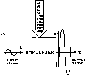
fig. 40
Using all the blocks which we came up to here we can now achieve a radio which would give us a reasonable sound also for stations which are not very near.
The result of the construction of a radio in that way would be a very simple radio receiver like it was built soon after the technology for amplifiers had been invented (the basics for this technology were the VALVES).
But very soon it was found that this simple construction had always a very high distortion, which was due to two reasons: So there was only one amplifier it was necessary in order to achieve a signal which was strong enough to have a very high AMPLIFICATION (the signal had to be enlarged very much in a simple amplifier circuit - called STAGE). Therefore it was necessary to have a signal as big s possible coming from the tuned circuits with a bad SELECTIVITY, which means they could not filter very exactly.
CONSEQUENCE: there are always radio stations transmitting on a carrierwave whose frequency is near to the frequency of the desired station, which reached the level of AUDIBILITY.
If a single amplifier stage has to amplify which very high amplification, it tends to produce oscillations itself, therefore it produces distortion itself. So the next step was to built in a second amplifier, but now one which was amplifying the still modulated signal appearing just out of the tuned circuit. This amplifier was called the RF-amplifier. The result was the a so-called TUNED FREQUENCY RADIO RECEIVER or TRF-receiver which was used from about 1930 till 1950.

fig.
41
6.7. SUPERHET RECEIVER (the SUPER)
The problem arising with RF-amplifiers in the TRF was: the RF-amplifier did not only amplify the desired signal of selected radiostation, but also to each additional signal, passing the tuned circuit.
So, by inserting the RF-amplifier the SENSITIVITY of the radio was improved (it could respond to weaker incoming signals too) but at the same time the SELECTIVITY (the ability to filter out a single radiostation only) was decreased, because now it could happen, that the speaker gave the sound of more than one radio-station at the same time.
The question was now: How is it possible to amplify (to add energy) the signal of the desired radiostation exclusively?
The answer was found in the beginning of the 40ties of this century. It was in physical sense the effect of SUPERHETERODYINING.
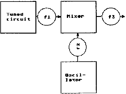
fig. 43
The function is in short like shown in fig. 42. The signal coming from the tuned circuit - from now on the RADIOSIGNAL (a) is mixed in a MIXER-STAGE with a RF-frequency signal supplied from the OSCILLATOR - from now on called the OSCILLATORSIGNAL (b) resulting at the end to a frequency f3 called the INTERMEDIATEFREQUENCY SIGNAL (c)
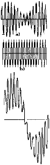
fig. 42
The oscillatorsignal is a signal with a constant frequency and a constant amplitude. You might assume that the oscillatorfrequency is desired to be exactly equal to the radio frequency in order to add energy to the incoming radiosignal.
For two reasons this is not true:
1. it would be very difficult to make sure that the oscillatorfrequency is exactly equal and in phase with the radiofrequency (if not phase, it would diminish the radiosignal).2. It has a very big advantage to mix with a frequency distant from the radio frequency but to keep the distance constant. This advantage will be cleared during the next chapter.
6.8 INCIDENTAL REMARK ON MIXING FREQUENCIES
If two signals with different frequencies are mixed in a MIXERSTAGE there will appear several new signals at the output: beside the two original frequencies we will find two new frequencies
fa = foscillator + fradio
fb = foscillator - fradio
for example:
In case of a wanted RF-signal of 1.52 MHz and an oscillator frequency of 1.976 MHz the frequencies fa and fb would be:
fa = 1.976MHz + 1.52MHz = 3.496MHz
fb = 1.976MHz - 1.52MHz = 0.456MHz
If we make sure that the distance between the frequency of the tuned circuit and the frequency of the oscillator is kept constant, we will find for every radiofrequency the same frequency at the output.
|
f1 (MHz) |
f2 (MHz) |
f3 (MHz) |
|
2.0 |
2.452 |
8.452 |
|
2.5 |
2.952 |
8.452 |
|
2.75 |
3.202 | |
|
3.01 |
3.462 | |
|
5.28 | |
8.452 |
| |
6.682 | |
| |
9.852 |
8.452 |
Therefore we will have at the output of the mixerstage always a constant frequency which is called now the INTERMEDIATE FREQUENCY which is derived from the oscillatorfrequency and the radiosignal and which is therefore still modulated with the audiosignal carried by the radiosignal. Figure 44. shows how this always constant intermediate frequency is achieved.
6.9. CONSTRUCTION OF A SUPERHETRADIO
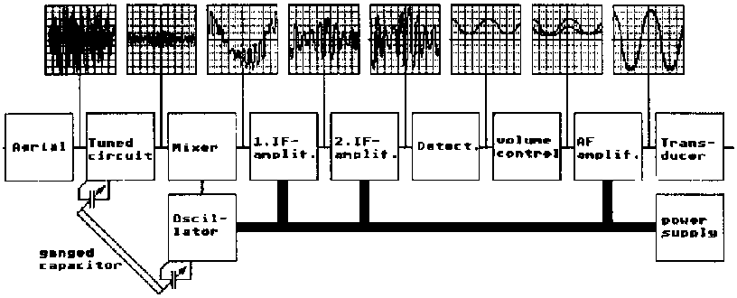
fig. 44
It is done by coupling two portions of a variable capacitor together. One of the portions is the part determining the frequency of the tuned circuit. The second portion is determining the oscillatorfrequency.
So both portions are changed strictly synchronically (they are turned by the same shaft) the frequency difference can be kept constant. This construction of a radio has several big advantages
1. The amplifiers amplifying the INTERMEDIATE FREQUENCY (called IF-amplifiers) can be tuned amplifiers which are tuned only to the very IF of this radio.
2. The energy of the desired radiosignal is increased very much, so that other stations fail the energy of “calling through” (being heard even though not desired).
SUMMING UP
We came to know now a series of different constructions of radios which have been invented step by step through the “history of radio technology”.
From step to step there was a technical improvement, always heading in direction to more sensitivity (being able to listen to distant stations) and more selectivity (being able to select only one station even if there are stronger stations near to the receiver) radios.
Fig. 45 to 47 should give you a general view about this development
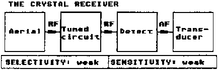
fig. 45
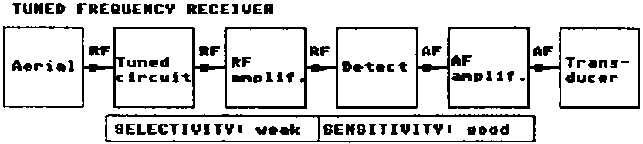
fig. 46
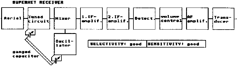
fig. 47
CHECK YOURSELF:
1. What is the function of the different blocks of a radio!
2. Explain how a tuned frequency radio receiver is made up!
3. How is a superhetradio working?
4. What is the advantage of a superhetradio compared with a TRF radio?
5. What is the IF? Where and how is it produced?
|
| |||||||||||||||||||||||||||||||||||
Radio and Electronics (DED Philippinen, 66 p.)
7. COMPONENTS OF MODERN RADIO RECEIVERS
7.1.1. HANDLING OF ELECTRONIC COMPONENTS
If you open a modern radio receiver, you will find, that all its components are extremely small. This is because the buyers of those radios want them to be as light as possible and the producers are trying to built them as cheap as possible.
To have light and small radios is on the one hand a big advantage. But on the other hand the tiny components, necessary for such small radios cause three major problems which you have to cope with if you want to repair this kind of radios instead of destroying them:
- small components have also a small mass. Small masses are heated up very easily. Most electronic components unfortunately are easily spoilt if they are heated up to much. Therefore while soldering in such radios you have always to take care,
- that the soldering iron is fitting for the job (as smaller the component, as smaller the iron).- that the soldering tin is fitting for the job (thin tin takes less time to get molten)
- that you never heat up the soldering point longer than necessary to limit the heat energy flowing to it, or
- if it is not possible to avoid heat, to cool the soldered terminal down by holding it by a pair of plier or touching it thoroughly with a screwdriver.
- small components have mostly very thin terminmalwires too, so you should always be extremly careful when bending or pulling any component in such a radio.- on an extremly small component you cannot write down any specifications. In order to enable you to find specification even though, there are used special colour codes. Generally you should not rub away any colour or letter on such a component. It might be you need this part of the specifications to repair the device properly.
7.1.2. HANDLING OF PRINTED CIRCUITS
Inside the radio you will find too that all the components are soldered to one or more sheets of brown or white plastic material which has on one or both sides copper or tinned conductor paths. These sheets are called PRINTED CIRCUITS. These plates are actually the whole wiring of this radio. To make it possible to have a rather complicated whole wiring on these sheets it is often necessary to print the conductorpaths extremly thin. This fact makes it necessary to keep in mind the following:
- Don't bend the printed circuits - you might break a single conductor and you hardly will be able to find this fault anymore.- heat them up only very carefully - you might destroy the conducting paths and then there is much more to be repaired than before.
- touch the conducting paths only if it is unavoidable-they might oxidate and then give no more good connection.
- if you want to check the circuit, always think about another method before starting to dissolder anything - you might spoil the conducting path.
- if you ever broke a conducting path you can repair it by a piece of wire (insulated or not depends on the case you find) but be careful not do cause a short circuit anywhere by a drop of tin (even a very small drop can cause a lot of trouble). In case of a short circuit you might spoil a few other components.
7.1.3. DIFFERENTIATION OF COMPONENTS
In order to be able to have a good general view of all electronic components we devide the whole lot into groups. The first of those groups is the group of PASSIVE COMPONENTS.
They are called passive, because they are only reacting on the signal connected to them. They do not control any other value. Examples of those passive components are the resistor, the capacitor, and the inductor. In most of those cases a passive component will have only two wires - but a few of the other groups have two terminals too. The second group of components are the ACTIVE COMPONENTS.
They are called active, because they control currents or voltages on their own, according to “orders”. Examples of those active components are diodes, transistors and thyristors. Except the diode all of them have more than two terminals.
|
| ||||||||||||||||||||||||||||||||||||||||||||||||||||||||||||||||||||||||||||||||||||
Radio and Electronics (DED Philippinen, 66 p.)
8. PASSIVE COMPONENTS
8.1. RESISTORS ELECTRICAL CHARACTERISTICS
voltage/ current relation:
The resistor allows a certain current to flow. According to OHMs LAW the current increases proportionally if the voltage is increased
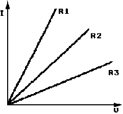
fig. 48
behaviour at changing frequencies:
if an ohmic resistor is connected across an alternating voltage of a varying frequency (while the amplitude of the voltage is kept constant) the current flowing will only depend on the voltage and the resistance of the circuit - not on the frequency.
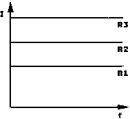
fig. 49
Main functions of Resistors in Electronics:
1. To control the amount of current flowing in a certain circuit (current path). Example: The current in the circuit will never exceed 40mA.2. To divide voltages in order to get certain partitions of the original voltage.
3. To translate currents into voltages and vice versa.
fig. 50

fig. 51
Makes of Resistors, used in Electronics:
In general there are two types of it; WIREWOUND and CARBONTYPE resistors.
Wirewound ones are mostly more expensive and need more volume. Therefore they are only used where extremly high powers have to be dissipated. For a power dissipation of less than 3 Watts there are almost exclusively used the so called MOULDED CARBON TYPE resistors. Clay, resin and carbonpowder is mixed in fitting proportions and then the whole mixture is poured into moulds and bibed at very high temperatures. Then the ends of the bodies are given a small metal solder contact at which the leads are bonded or soldered. Mostly those resistors get additionally an insulating cover and the specifications are printed on that cover - Either in form of numbers and letters or in form of colour rings.
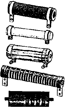
fig. 52
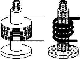
Nowadays those resistors are manufactured at a very good standard and most of them within a tolerance of five per cents. It would be not economical to produce them with each and every resistance (like 101, 102, 103 Ohms and so on). Instead of that, they are produced in special rows. The most often appearing row is the so called E 12 series. The specification E 12 means: we find per decade 12 different values each of it having a resistance of about 20% higher than the smaller one (100, 120, 150, 180 and so on).
example:
2 decade: 10/12/15/22/27/33/39/47/56/68/82/103 decade: 100/120/150/220/270/330/390/470/560/680/820/1000
and so on......
CHECKING AND HANDLING OF RESISTORS IN ELECTRONIC EQUIPMENT:
If you measure the following values:
You can assume:
No voltage across the resistor while the supply is on:
Either a short circuited resistor or an open circuited one.
A voltage very similar to the supply voltage at a resistor which is connected in series with other resistors:
Either the other resistor is short circuitedor the measured one is borken.
HOW TO REPLACE RESISTORS?
Make sure that the new resistor has:
- the same RESISTANCE and
- the same or a higher power rating.
If you don't have the fitting values available there are possibilities to achieve the intended values by series or parallel connections (but check if the power rating of your resistors is fitting).
VARIABLE RESISTORS
At certain points in a radio we find resistors of which the resistance can be changed. We call them “variable resistors”. The resistance between certain terminals of these resistors can be variated by sliding a slider over the resistor. These variable resistors can be of two different groups:
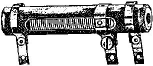
fig. 53
ADJUSTABLE RESISTORS are variable resistors whose slider can be moved only by means of a screwdriver. Those resistors are normally fixed at positions where under normal service conditions you cannot reach. They are meant for setting the circuit to special values before it is handed over to the customer. During normal service they are not touched anymore.

fig. 54
VARIABLE RESISTORS
(real ones) can be operated by turning a control knob or a control slider and they are fixed so, that the customer can reach them anytime he wants to.
These variable resistors are produced in two different types.
Very often the resistance (wire or moulded carbon) is brought on to the body of the resistor, so that the resistance is changing proportionally to the distance which the handle is moved over the resistor. These types are called the LINEAR VARIABLE RESISTORS.
For special purposes it is sometimes necessary to have a different behaviour of the resistance when moving the slider. For volume controls for example, the LOGARITHMIC VARIABLE RESISTOR is used, because the (turning it halfway seems to decrease the sound for fifty per cent, even though the resistance value has been increased four times).
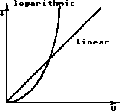
fig. 55
EXERCISE:
You want to know the current flowing in a resistor on a printed circuit.
You do not want to dissolder the component (because of the reasons explained above).
Therefore you are intending to use an oscilloscope and you want to measure the current indirectly. You find - with setting of the controls as shown in the following figure - a signal as shown on the screen.
The resistor has the following colour rings.
A- gold / B- red / C-green / D- brown.
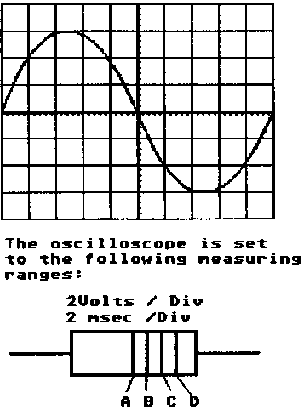
fig. 56
QUESTIONS
1. What is the resistance of the resistor?
2. What is the peak to peak voltage at the resistor?
3. What is the rms value of the voltage at the resistor?
4. What is the current flowing through the resistor which you would measure at a analogue multimeter if you would dissolder one terminal of the component?
8.2. CAPACITORS
ELECTRICAL CHARACTERISTICS
A) capacitors at dc
EFFECT: If we connect a capacitor to a dc voltagesource there will flow a considerable high current in the first instant. But this current will decrease fast, to lower values and it will be 0 after a relatively short time.
REASON: When first connected to the dc-voltage, the charge on the capacitor is 0. Therefore the voltage source will start to charge the capacitor. The charges brought to the capacitor are electrons pushed to the negative plate, and electrons sucked out of the positive one. As soon as the plates have a charge big enough to stand for the same voltage as it has the source, there is no more potential difference and therefore the current in the circuit must be 0 again.

fig. 57
B) capacitors at ac
EFFECT: For easier understanding let us first imagine not a sinusoidal alternating voltage but a FLAT-TOPPED AC-VOLTAGE one. (This means nothing else than a dc voltage whose polarity is changed over after a certain period of time). In this case we can easily imagine, that there will be a charge current at each change of polarity.
RESULT: There flows a current always if there is a change of voltage.
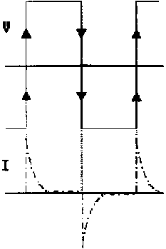
fig. 58
Now let us observe a SINUSOIDAL AC VOLTAGE:
- After having had a closer look to that ac-voltage we will find, that it is changing all the time except of the two instants at the peaks.- Applying the results of the findings at the flat-topped ac-voltage we can foresee that the current will now flow all the time because the voltage changes constantly.
- If we have understood that the current flowing in this circuit is depending on the change of the applied voltage we can easily predict, that the amount of current flowing will depend on the velocity of voltage change. (as faster the voltage will change as higher will be the current flowing).
-Applying these modified findings, we can conclude, that the current will have its maximum when the voltage is changing at its fastest rate - and this is the fact at the noughtpoints of the ac-voltage.
Of course between the four points found with the considerations above there are values of the current which form altogether a sinewaveagain. These considerations enable us to explain now two characteristics of an ac-current flowing through a capacitor.
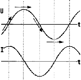
fig. 59
PHASE RELATION
As we see the current is always flowing “earlier” than the voltage is arising.
The current is phase-shifted in relation to the voltage. The current is LEADING
The biggest phases-hift possible is a quarter of a period (or 90 degrees).

fig. 60
FREQUENCY RESPONSE
As we found - the current depends on the change of voltage.
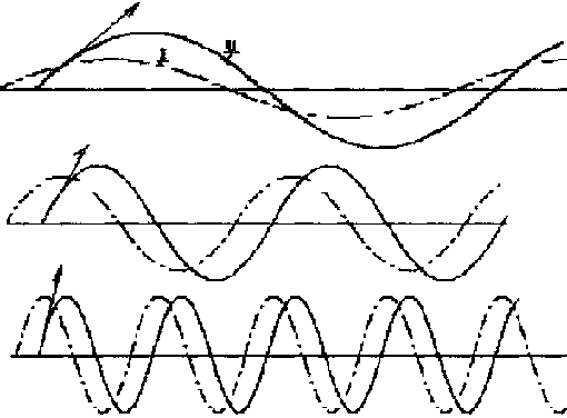
fig. 61
If we compare now two different frequencies with the same amplitude of voltage we can see, that at a higher frequency the change of the voltage must be around the noughtpoint higher than at a lower frequency.
This observation makes it clear that the current at a higher frequency will be higher and therefore we can derive that the ac-resistance which is called IMPEDANCE OF A CAPACITOR IS AS LOWER AS HIGHER THE FREQUENCY CONNECTED IS.
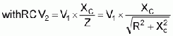
IMPEDANCE/CAPACITIVE REACTANCE
The impedance of a capacitor can be calculated by the formula:
|
|

Whereby R is the OHMIC RESISTANCE which is causing “losses” and X is the so called CAPACITIVE RACTANCE which is to be calculated by the formula:
|
|

MAIN FUNCTIONS OF CAPACITORS
1. To smoothen the pulsating currents in power supplies. You can also say to “short circuit” ac-components within pulsating dc-voltage. SMOOTHING CAPACITORS
fig. 62a2. To block dc-voltage and to let ac-curents flow from amplifier to amplifier stage. COUPLING CAPACITORS.
fig. 62b3. Combined with resistors we find them in so called PASSES which let only pass special frequency ranges.
fig. 62c4. in combination with inductors for TUNED CIRCUITS, which filter out special frequencies from a certain mixture of signals.
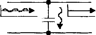

fig. 62d
KINDS OF CAPACITORS
POLYESTER CAPACITORS have almost replaced paper capacitors. They are made in values of 0.01 mikro Farad up to 10 mikro Farad. They are for general purpose use.
MICA CAPACITORS are used in RF circuits and are made in values up to 0.01 mikro Farad.
CERAMIC CAPACITORS have an extremly constant capacity. They are consisting of a ceramic chig which has a layer of metla on both sides.
ELOCTROLYTIC CAPACITOR are made by putting an oxide layer on the surface of an aluminium foil. The other plate of the capacitor is formed by an electrolyte in which the foil is emersed after having been rolled. The oxide is the dieelectric. They are polarized and may exclusively be connected in the fitting direction otheriwse they might explode.
VARIABLE AIR DIEELECTRIC CAPACITORS consist of tow groups of plates made from aluminium sheets. One of the groups is fixed the other one is movable. They can be moved in and out and so change the capacity of the capacitor. They are used only for tuned circuits.
CHECKING AND HANDLING OF CAPACITORS IN RADIO SETS.
Big capacitors are almost always smoothing capacitors and therefore it is possible to measure the voltage at them. It should be under normal conditions near to the supply voltage.
With smaller capacitors it is not possible to measure the voltage, there you can only measure if the capacitors has a high resistance for dc.
If you have to replace a capacitor you have to observe two values:
1. the voltage rating: capacitors are limitted in voltage applicable to them. If there is no fitting replacement. You can connect them in series2. the capacitor If you don't have a fitting one you can arrange one by connecting several in parallel but keep in mind the voltage rating.
To find the values of a special capacitor you will find either the specifications printed on them, or you find the colour code system, whereby the value found out is in piko Farad.
CHECK YOURSELF:
1. How is a capacitor behaving at dc or ac?
2. How is the phase relation between voltage and current at ac?
3. How is the influence of the frequency on the impedance?
4. What does the term impedance mean?
5. What does the term reactance mean?
6. Which different functions can capacitors be used for in radios?
7. Which different kinds of capacitors for you know
8. What to do in order to check a capacitor in an electronic device?
9. What is necessary to be kept in mind if you want to replace a capacitor.
8.3. INDUCTORS
ELECTRICAL CHARACTERISTICS OF INDUCTORS
A) Inductors at dc
If we connect an inductor to a dc-voltage-source we will find: it takes some time till the current has reachted its full value. The amount of current flowing at last will be depending only on the voltage connected and the ohmic resistance (the resistance of the wire).
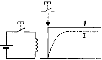
fig. 63
B) Inductor at ac
If we connect the same inductor to an ac-voltage of the same magnitude than the dc was, we find a much smaller current flowing.
We know, that the resistance of the copperwire will not have changed. But we know too, that in every circuit the current is governed by Ohm's Law.
So the decreased current is only possible if the ac-voltage has somehow decreased in the circuit.
We know too that in a coil in case of change of current is produced a so called BACK-EMF.
Applying this knowledge we can assume the shape of the back emf. It will be slightly smaller but exactly inverse to the original voltage. The rest of the voltage left over is necessary for the resistance of the copperwire. We know too that the amount of back emf is depending on the change of current in the coil. Applying this we can state: the current must have its fastest changes when the back emf has its maximum. So the back emf has an opposite direction the current must change positively to produce a negative back emf and vice versa. Also we can state: the current must not change anyhow while the back emf is “0”. We have got now four conditions for the shape of the current flowing in the circuit of an inductor connected to an ac-voltage. We can easily foresee, that the current will flow in the shape of a sinewave.
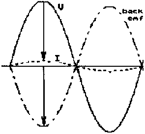
fig. 64
We can also predict some facts about the phase relation between voltage and current.
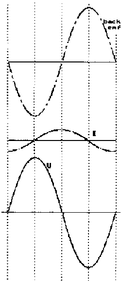
fig. 67
PHASE RELATION
As we concluded above at an inductor the current must be LAGGING BEHIND THE VOLTAGE. The biggest phaseshift possible is 90 degrees. But this value cannot be reached in practice.
FREQUENCY RESPONSE
As we found the back emf depends on the change of the current. If the frequency of the sinewave is higher we will find a faster change of current, and therefore there will be produced a bigger back emf.
So we can derive: as higher the frequency as lower will be the current - this means as higher the frequency as higher the impedance of the inductor.
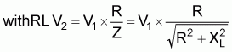
The impedance of the inductor is to be calculated by the formula:

And the inductive reactance of the inductor can be calculated by the formula:

MAIN FUNCTIONS OF INDUCTORS
Inductors can be divided into two main groups:
A) LOW- (or audio-) FREQUENCY INDUCTORS. They are used for smoothing the dc of the supply or for letting through only audio frequency and to cut off high frequencies.
fig. 68B) HIGH- (or radio-) FREQUENCY INDUCTORS They are used in tuned circuits and for aerial coils onferrite rods. They are small compared with those of group A and often they do not even have an ironcore.
figureIf the frequency is very high the wires are mode out of a lot of extremly thin strands in order to avoid the so called “skin effect”.
SPECIALITIES:
A) Sometimes we find in superhet receivers for cars instead of variable capacitors so called variable inductors used for the tuned circuits.B) To cut off very high frequencies in wires entering a special part of a radio or another electronic equipment, there are used simple pearls of ferrite which are just put on the wire.
CHECKING AND HANDLING OF INDUCTORS
The possibilities to check an inductor by simple means are very limitted.
With a normal AVO-meter we can just measure the ohmic resistance across the two terminals. But we will hardly read more than 10 Ohms. Mostly we will measure values near “0” Ohms and if we find that, we can be sure that the wire is at least not broken, but we do not know
- if there is short circuited winding, or
- if there is anything wrong with the ironcore.
These kinds of faults can cause very considerable changes of the inductivity of the inductor.
If we suspect a fault like that we can only replace the inductor by one of the same type, or we have to measure the impedance of it at the frequencies it is meant for.
PLEASE KEEP IN MIND: There are always found inductors with an iron core which resembles a screw. They are meant for adjustment but....
NEVER TRY TO ADJUST THESE INDUCTORS ONLY FOR FUN AND WITHOUT MEASURING THE SIGNALS PRODUCED! YOU WILL MISALIGN THE RADIO!!
NEVER TOUCH THE IRON CORES WITH A NORMAL SCREWDRIVER. YOU MIGHT MAGNETIZE IT, AND THAN IT WILL NOT WORK PROPERLY ANYMORE.
CHECK YOURSELF
1. What are passive components
2. Compare the behaviour of a) resistors, b) capacitors, d) inductors at ac voltages with different frequencies.
3. Explain the term phaseshift and state which kind of phaseshift we find at a) resistors, b) capacitors and c) inductors.
8.4. COMBINATION OF PASSIVE COMPONENTS
8.4.1. SERIES CONNECTION OF R AND C, OR R AND L
If a series connection of a resistor and a capacitor, or of a resistor and an inductor is connected across an ac-voltage they stand for two different impedances. Leaving aside that the capacitor and the inductor have always a small ohmic resistance, we can simplify the situation by looking at them at first as solely capacitive or inductive reactances Xc or X1.
Recollecting our knowledge about phase relations at L and C, we find that the voltages appearing in the circuits shown in fig. 69 must have special relations. As we know:
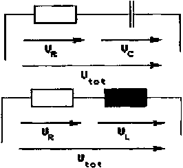
fig. 69
In a series connection of resistances the curent in both components is equal.
Intending to draw a phasor diagram we start therefore with the phasor of the current Itot. We know in both circuits the voltage at the resistor Vr must be exactly in phase with that current.
While the voltage at the capacitor must be lagging for 90 degrees in relation to the current and the voltage at the inductor must be leading for 90 degrees. As we know too: phasors are added geometrically.
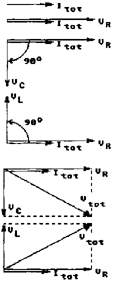
fig. 70
Therefore the overall voltage Vtot will be found by shifting the start of Vr up to the end of Vc or V1 and by drawing a line from the noughtpoint up to the end of Vc or V1 we get the overall voltage Vtot necessary to let the current Itot flow through the circuit.
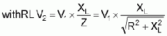
The voltages found at those components are depending on Ohm's Law, therefore Vr = I x R, Vc = I x Xc, and V1 = I x X1
These formulas demonstrate too: the relation between the voltages is equal to the relation between the reactances. In order to get an imagination of the behaviour of one of those circuits we can therefore draw instead of the voltage-triangle a triangle made up from the resistance, the reactance and showing the overall impedance.
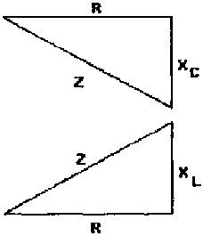
fig. 71
This triangle shows very clearly: the impedance of the circuit can be calculated by using the old formula of PHYTHAGORAS. This combination introduced here can be used for so called PASSES.
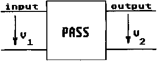
fig. 72
If we observe how the OUTPUT VOLTAGE is changing while the frequency of the INPUT VOLTAGE is increased over a certain range we observe that the output voltage is:
- either changing from low to high values (HIGH-PASS)
- or from high values to low values (LOW-PASS)
The combination of R and C or R and L offers four different possibilities depending on where the components are positioned.
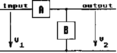
fig. 73

fig. 75a
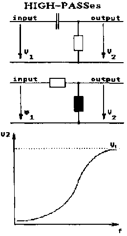
fig. 75b
As we can see from the graphs showing the outputvoltage is not suddenly cut off totally at a special frequency, but the outputvoltage is fading out over a wide range of frequency.
We can calculate the output-voltages at various frequencies at each PASS-combination by the following formulas:
|
“HIGH” - Passes |
|
|
|
|
|
“LOW” - Passes |
|
|
|
|

Nevertheless for technicians it is necessary to compare different passes in relation to their ability to pass or to cut off the input signal.
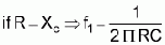
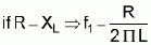
Therefore there was defined a certain “LIMITTING FREQUENCY” which is considered as the frequency from which on the output-voltage is defined as “cut-off”. This limitting frequency is reached if the output-voltage is equal or lower than 70.7% of the input-signal. This limiting frequency can be calculated by the following formulas:
|
limit frequency |
limit frequency |
|
|
|
CHECK YOURSELF.
1. What does the term PASS mean 7
2. What is the difference between a HIGH - and a LOWPASS.
3. An RL Highpass should have a limitting frequency of 120 Hz. You have a coil with 150 mH. What is the resistance necessary for this pass.
4. What is the limitting frequency of a Low pass which is consisting of a resistance R=120 Ohms and a capacitor of 2 mikroFarad?
5. The limitting frequency of an amplifier should be 28 Hz. The coupling-capacitor. The coupling-capacitor has a capacity of 4.7 nF. Which resistance must have the resistor?
8.4.2. COMBINATION OF L AND C, RESONANT (TUNED) CIRCUITS
Combinations of inductors and capacitors have always a special characteristic referring to their RESPONSE to different frequencies. If we want to understand their behaviour we have two main possibilities:
FREE OSCILLATING CIRCUIT
Let us suppose a capacitor is charged with a certain voltage. As soon as this capacitor is connected across an inductor there starts to flow a current. The amount of current is slowly increasing because of the self-induced voltage across the coil.

figure
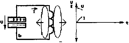
figure
figure
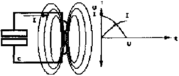
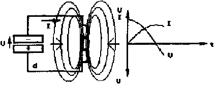
On the one hand this current is discharging the capacitor which lets drop the voltage of the capacitor. On the other hand the increasing current is building up a magnetic field around the coil. The current will reach its maximum just when the capacitor is discharged totally. At that very instant the voltage at the capacitor is Cero while the current is at its maximum, and therefore the magnetic field has its maximum too.
figure
There is no charge left at the capacitor, therefore the capacitor cannot deliver any current anymore. Combinations of inductors and capacitors have always a special characteristic referring to their RESPONSE to different frequencies. If we want to explain their behaviour we have two main possibilities:
FREE OSCILLATING CIRCUIT
Let us suppose a capacitor is charged with a certain voltage.
As soon as this capacitor is connected across an inductor there starts to flow a current. The amount of current is slowly increasing, because of the selfinduced voltage across the coil.
On the one hand this current is discharging the capacitor which lets drop the voltage of the capacitor. On the other hand the increasing current is building up a magnetic field around the coil.
The current will reach its maximum just when the capacitor is discharged totallyted across an inductor.
At that very instant the voltage at the capacitor is Cero while the current is at its maximum, and therefore the magnetic field has its maximum too.
There is no charge left at the capacitor, therefore the capacitor cannot deliver any current anymore. The current will have to vanish, but it will not stop to flow immediately. As soon as the current will be Cero the magnetic field must have vanished too. But before this can be the case, the magnetic field has to collapse first. The collapsing field will induce a voltage across the coil which will have a direction opposite to the voltage connected to it when the current started to flow.
This selfinduced voltage will cause a current to flow. This current will have the same direction as before, and it will charge the capacitor again but now in opposite direction.
As soon as the magnetic field has vanished totally the capacitor will be charged again to a voltage of the same amount as it was in the beginning, but in opposite direction.
Now the same process will start again, and cause a second halfwave of a sinusoidal ac-current and voltage. Summarizing: If we inject some electric energy to a parallel connection of a capacitor and an inductor there will appear an ac-voltage across the circuit with a frequency depending on the inductance and on the capacity.
But in reality these oscillations will fade out very soon, because the current flowing in this circuit to and for has to pass some obstacles. So for example the resistance of the wires forming the coil, or the resistance of the interconnecting wires. There will vanish also some of the charges stored in the capacitor by moving through the insulating dieelectricum.
All in all, after a short time we will find no more oscillations.
We can explain this effect also from another point of view:
ENERGY CONSIDERATIONS
If we look at the process explained in the last chapter from the point of view of energy, we will find that this LC combination is behaving very similar like a pendulum.

fig. 77
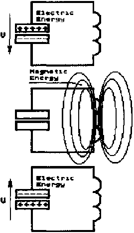
fig. 78
A pendulum starts with a lifted mass which means there is POTENTIAL MECHANICAL ENERGY
When released, the mass gains more and more velocity during its movement downward to the lowest point. In terms of energy: the potential energy is turned into CINETIC ENERGY.
This cinetic energy will cause the mass moving on upwards after passing the lowest point and - by moving upward again - turning the cinetic energy back into POTENTIAL MECHANICAL ENERGY.
TUNED CIRCUIT
Starts with seperated charges on the plates of the capacitor which means ELECTRIC ENERGY.
Once connected to the inductor, the capacitor starts to discharge and push current through the inductor. The current will cause a magnetic field in the inductor and - as soon as the capacitor is totally discharged - the former electric energy is turned into MAGNETIC ENERGY.
So the capacitor is free of charges now, it cannot supply any current anymore, and therefore the magnetic field starts to collapse now.
The collapsing magnetic field induces a voltage and causes the current to go on flowing as before.
This will charge the capacitor no in opposite direction as before. This effect goes on till the capacitor is charged again and the magnetic field has been turned into ELECTRIC ENERGY again.
CHECK YOURSELF:
1. Describe the construction of a tuned circuit.
2. Describe what happens in such a circuit after some energy into it.
3. Explain the similarities between pendulum and resonant circuit.
4. What is the reason for the fast vanishing of oscillations in such a circuit?
8.4.3. TUNED CIRCUIT CONNECTED TO AN AC-VOLTAGE
SERIES TUNED CIRCUIT AT AC
If we connect an ac-voltage source across an LC combination as shown in fig. 79 This can be looked at as a series connection of two impedances connected to an ac-voltage source.

fig. 79
To simplify the problem we can ommit first the ohmic parts of the two components and concentrate on the reactances only. We know, that their reactances are depending on the frequency of the voltage they are connected to. Refering to a series connection of resistors and the rule, that the overall resistance of two resistors connected in series is the some of the two original resistances, we can easily derive that the overall impedance of that series connection will be the sum of the two original reactances.
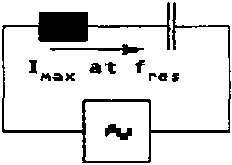
fig. 80
If we do the addition of the two reactances by graphical means, as shown in fig. 80 we find, that the overall impedance will have high values at deep and at high frequencies, and it will have a minimum at a certain frequency. This certain frequency is called the RESONANT FREQUENCY or the TUNED FREQUENCY and it will be exactly that frequency at which the reactance of the inductor and the reactance of the capacitor will be equal. Summing up our findings we can also say: the current in this circuit will be maximum at the resonant frequency.
PARALLEL-TUNED CIRCUIT AT AC
If we want to derive, what happens in a parallel combination of an inductor and a capacitor, connected to an ac-voltage (as shown in fig. 81), we can again use the graphical method.
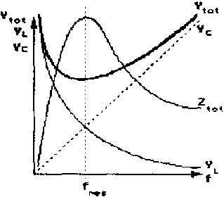
fig. 81
But this time we have to add the ADMITTANCES of the reactances of the two components to find the overall admittance in that circuit.
The admittances equal the reciprocal of the reactance. Adding the values of the admittances we get as the overall admittance Ytot. But we should not forget, that this represents the overall admittance, and in order to be able to compare it with our findings in the chapter before we have to turn this graph into a graph representing the overall impedance which is again the reciprocal value of the admittance. The result is shown in fig. 81. And we find that here the impedance has a peak value exactly at the so called resonant frequency.
SUMMARIZING
SERIES TUNED CIRCUITS HAVE A MINIMUM IMPEDANCE AT RESONANT FREQUENCY!
PARALLEL TUNED CIRCUITS HAVE A MAXIMUM IMPEDANCE AT RESONANT FREQUENCY!
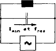
fig. 82
THE RESONANT FREQUENCY
Up to now we do not know, how to calculate the resonant frequency, for any combination of an inductor and a capacitor. As we stated above, the resonant frequency appears if the reactance of the inductor equals the reactance of the capacitor.
Therefore it is easy to derive the formula for the resonant circuit.


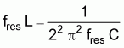
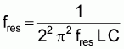


8.4.4.1. QUALITY OF TUNED CIRCUITS
For radio technology tuned circuits are mainly means to filter out a special frequency from a spectrum of frequencies. Therefore radio technicians would wish it would be possible to construct tuned circuits with a graph as shown in fig. 83. A tuned circuit with such a characteristics gle frequency. But a tuned circuit in reality will never have such a characteristics. Its characteristics will always be much smoother.
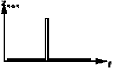
fig. 83
But different combinations of different inductors and capacitors, will show different characteristics. And it is now necessary to differentiate them.
To find out the quality of a tuned circuit mostly we use a connection like shown in fig. 84. If we vary the frequency of the ac-source we will measure changing voltages at the voltmeter. This can be understood very easy if we look at the circuit as a series connection of a resistor and a tuned circuit of parallel type.
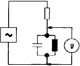
fig. 84
Recollecting the overall impedance of the parallel type we can easily predict that the current at resonant frequency will be minimum and therefore the voltage V at the Voltmeter will be maximum. If we plot these values, we find also for the resonant frequency certain resistance in the tuned circuit. This resistance is called the RESONANT RESISTANCE.
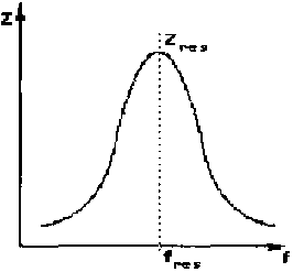
fig. 85
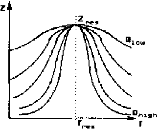
fig. 86
If we imagine we would connect additional resistances in parallel and we would repeat the same experiment, we can predict too, that the graphs get as flatter as lower the parallel resistance gets. A flatter graph shows that the circuit is less able to filter. The QUALITY of tuned circuits can be calculated by the following formulas:
|
parallel Tuned circuit:
series Tuned circuit:
|


8.4.4.2. BANDWIDTH
Sometimes it is important to have a tuned circuit which lets through not only a single frequency, but a whole bond of frequencies. In this case it could be important to have a flatter graph. To be able to define the bandwidth of tuned circuit, there is again taken the value of 0.707 as limit. This means it the output voltage has dropped to 70.7 % of the output at fres the limit is reached.
CHECK YOURSELF
1. What is the difference of a series and a parallel tuned circuit?
2. What is the meaning of the terms: resonant frequency. Quality, bandwidth?
3. You have found in a radio a parallel connection of a capacitor of 10nF and an inductor with 100mH. What is the resonant frequency?
4. You want to built a tuned circuit for MW. You have a variable capacitor of 500pF. What inductance must the coil have? (500pF is the maximum value of the variable capacitor).
|
| ||||||||||||||||||||||||||||||||||||||||||||||||||||||||
Radio and Electronics (DED Philippinen, 66 p.)
9. ACTIVE COMPONENTS -1- DIODES
9.1. CHARACTERISTICS OF SEMICONDUCTORS
As already stated in chapter 7.1.3 active components can be valves or semiconducting type. In this script we will deal only with the modern type: the semiconductor active components. To understand the function of these components it is necessary to have some basical knowledge of semiconducting materials and how they are processed in order to produce the type of active component desired.
9.1. CHARACTERISTICS OF SEMICONDUCTORS
Wellknown Semiconducting materials are: germanium, silicon and selenium. All of them have exactly FOUR VALENCE ELECTRONSTRONS.
fig. 86a
To purify those materials they are first molten in order to get rid of any other type of atoms. During cooling them down again, the atoms form compounds in which always two “neighbours” use two of their electrons “together”. That means: those two electrons could be found on both atoms. This scheme is represented in fig. 86b. In this figure we realize as well: only within this structure the centre atom has eight valence electrons now, and this means in chemical sense it is “saturated”.
fig. 86b
A whole crystal of these atoms would look like fig. 86.c
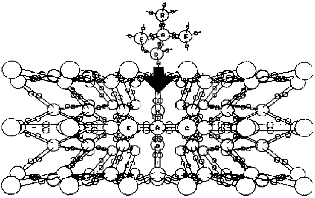
fig. 86c
At cero degrees Kelvin a piece of this type of material has no free electrons, and therefore no free chargecarriers ® infinite resistance (remember the difference at metals: they have the lowest possible resistance at this temperature).
In order to make further drawings concerning semiconductors more easy to understand we will simplify the structure shown in fig. 86d and show only two dimensions in fig. 86e.
fig. 86e
As a crystal-structure this looks now like fig. 86f.
fig. 86f
INTRINSIC CONDUCTION
If this material is now heated the whole structure is moving - as hotter as faster! This will cause some of the electrons to loose “contact” to their related atoms and therefore they are released to move through the material. As there are now free chargecarriers there will arise conductivity now and this is called INTRINSIC CONDUCTION. This effect is represented in fig. 86g.
fig. 86g
HOLES-GENERATION RECOMBINATION
If there is released an electron anywhere there is not only created a free negative chargecarrier but at the same time there is left back in the atomic structure a positive charge - a so called HOLE. The effect through which the hole and the free electron are created is called GENERATION.
The hole now again will attract any electron in its surrounding. Therefore at the same time when generation takes place another opposite effect happens too: the return of an electron to a hole, and this effect is called RECOMBINATION.
SUMMING UP:
SEMICONDUCTORS HAVE INFINITE RESISTANCE AT 0 DEGREES KELVIN.
WHEN HEATED UP, THERE ARE CREATED MORE AND MORE CHARGECARRIERS WHICH MEANS: THE CONDUCTIVITY OF THE MATERIAL IS INCREASING WITH INCREASING TEMPERATURE.
DOPING
As you might know already: one of the advantages of semiconducting active components is, that they are not depending on heat (as valves do). So for normal components there must be something done, to get them conducting reasonably at normal temperatures. Therefore now some atoms of another type will be implanted by purpose to the pure semiconductor. The process to do this under controlled conditions is called DOPING. It is done with two types of foreign atoms.
THE N-TYPE MATERIAL
Doping with atoms five with valence electrons leaves one of the five atoms of the foreign atom here arsenic free. As this electron is not related to any other part of the structure it is free to move, and it can carry now electricity.
fig. 86h
If we look at this doped material from a more general point of view. We can forget about the structure of “normal-semiconducting-atoms” and only see it as represented in fig. 86h as a material with:
POSITIVE CHARGES which are FIXED here within the atomic structure, and NEGATIVE ELECTRONS which are FREE to move.
THE MATERIAL CREATED BY DOPING WITH ATOMS WITH FIVE VALENCE ELECTRONS IS CALLED:
N-TYPE MATERIAL.
THE P-TYPE MATERIAL
Doping with atoms with three valence electrons leaves one of the links between the other atoms and the foreign atom (here indium) free.
As always at normal temperatures generation takes place this gap will be filled by such a generated electron. But this leaves back a hole which can move now, in the following way: the next generated electron in the surrounding will leave back another hole and on the other hand fill this hole. In this manner the hole has been moved.
So we have now holes as free chargecarriers.
figure
fig. 86i
figure
If we look at this doped material from a more general point of view. We can forget about the structure of “normal-semiconducting-atoms” and only see it as a material with:
NEGATIVE CHARGES which are FIXED here within the atomic structure, and POSITIVE HOLES which are FREE to move.
THE MATERIAL CREATED BY DOPING WITH ATOMS WITH THREE VALENCE ELECTRONS IS CALLED:
P-TYPE MATERIAL.
BUT KEEP IN MIND: even after doping the material as a whole is still electrically neutral.
9.2. THE PN-JUNCTION OR DIODE
The next step of explanation is a totally theoretical one, because in reality a material with two zones - a N-type and a P-type one - is created in practice by doping with from two opposite sides with two different materials.
But in order to understand the effect, it will be imagined here, that both types are ready prepared and then brought together. As soon as they are near to each other the free chargecarriers near to their border will move in direction to each other as shown in fig. 86 j.
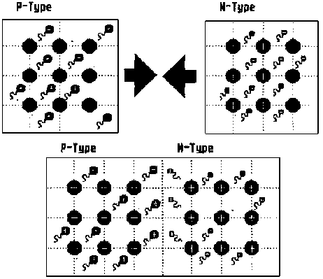
fig. 86j
Of course will the positive and the negative chargecarriers meeting at the border at once cancel each other.
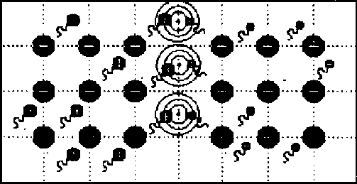
fig. 86k
But the cancellation of chargecarries on each side will leave the opposite chargecarriers belonging to them back. This will lead along the border to a so called SPACE-CHARGE-REGION, which is represented in fig. 86 l (top).
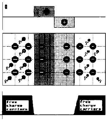
fig. 86l
This space-charges prevent now the free charge carriers from both sides to cross the border and to go on cancelling eachother.
At last there will appear a voltage across this border which is depending on the material used. So the intruding of the chargecarriers from one side to the other is called DIFFUSION this voltage is called DIFFUSION POTENTIAL. In technical sense it will be called THRESHOLD VOLTAGE (Ge = 0.2 V/Si = 0.7 V)
As we derived above, the free chargecarriers around the border cancelled eachother. This leaves on the other hand a zone in which we will find no more free chargecarriers a so called DEPLETION ZONE (Depletion means to get poor). From the point of view of conductivity means this:
THIS ZONE HAS NO CONDUCTIVITY AND AN ALMOST INFINITE RESISTANCE.
9.2.1. PN-JUNCTION CONNECTED TO VOLTAGE
Up to this point, there was nothing connected to the PN-junction. Now we have to consider, what will happen at this junction if we connect a voltagesource to it.

fig. 86m
If we connect the positive pole of the source to the N-type side and the negative pole to the P-type side, we can imagine the positive pole attracting the free electrons of the N-type side, and the negative pole attracting the holes of the P-type side, and so on both sides reducing the number of charge carriers there as shown in fig. 86 n.
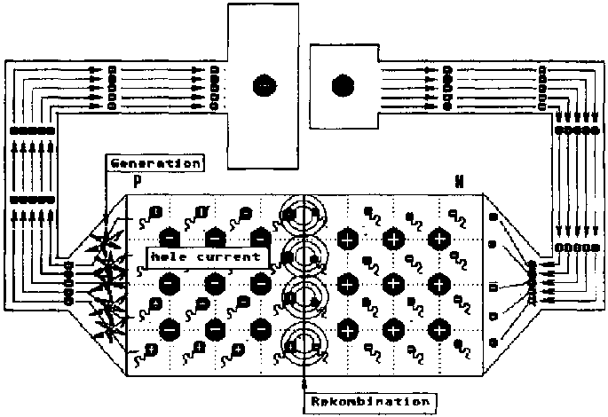
fig. 86n
This effect extents the depletion layer. Therefore the resistance of the junction is increased and therefore
IN REVERSE DIRECTION THERE WILL FLOW NO CURRENT.
FORWARD VOLTAGE
If we connect the negative pole of the source to the N-type side and the positive pole to the P-type side, we can imagine the positive pole repelling the free holes of the P-type side in direction of the border, and the negative pole repelling the electrons of the P-type side in direction of the border.
So the charge carriers are invading the depletion layer it-will get conducting. Therefore the resistance of the junction is tremendously decreased and their depletion layer vanishes. IN FORWARD DIRECTION THERE WILL FLOW CURRENT.
9.2.2. CHARACTERISTICS OF A PN-JUNCTION OR DIODE
The behaviour of such a junction as explained up to here would look like fig. 89 a. If we look at it from a general point of view we find on the left side (at reverse direction) no current at any voltage (infinite resistance) and on the right side (forward voltage) no voltage necessary for any current (no resistance).
fig. 89a
We see: this component behaves like a valve which lets flow current only in one direction. The symbol is shown in fig. 89b. It is called a DIODE and its terminals are called ANODE and CATHODE (these terminals are originated from the valve diode).

fig. 89b
But the characteristics shown in fig. 89a is only a theoretical one. We can use this imagination for simple considerations in circuits with diodes.
In reality the characteristics is shown in fig. 89. The difference is:
- in reverse direction exists a voltage-limit.If we increase the reverse voltage above this limit there will flow suddenly a strong current which will destroy the diode at once. This limitting voltage is called BREAK THROUGH VOLTAGE.
- In Forward direction at first a voltage is needed to get any current flowing, this voltage was mentioned already above, and it is called the: THRESHOLD VOLTAGE.
- Additional the diode still needs some voltage to let flow some forward cur rent which means it has a certain resistance which is called INTERNAL RESISTANCE

fig.
89c
9.2.3. ZENERDIODE
There are special diodes which are not destroyed if connected in reverse direction if the voltage is reaching the break down voltage. This type of diodes is called zenerdiode and it is used for stabilization. Its symbol and characteristics is shown in fig. 89d.
fig.
89d
|
| |||||||||||||||||||||||||||||||||||||||||||||||||||||||||||||||||||||||||||||||||||||||||||||||||||||||||||||||||||||||
Radio and Electronics (DED Philippinen, 66 p.)
10. BLOCKS OF RADIOS / -1- / POWER SUPPLIES
10.1. GENERAL CONSIDERATIONS
Kind of supply voltage:
Radio receivers like most of the electronic nowadays need for good performance a -dc-voltage which is very stabil.
Reason:
Every change of the supply voltage acts on the receiver like an injected signal and this means distortion.
Energy source:
Nowadays mostly batteries or powersupplies from mains.
Amount of supply voltage:
Depending on the kind of “active-components” used in the receiver. For valve receivers “high tension” (75 - 350 V), for transistor receivers (3 - 24 V).
Stages in a power supply:
According to the problems arising in a special case, there are different stages necessary in a power-supply in order to have the constant dc-voltage required.
|
Energy source |
stages required |
kind of radio supplied | ||||
|
mains |
--------- |
transforming |
rectifying |
smoothing |
stabilizing |
working |
|
batteries |
chopping |
transforming |
rectifying |
smoothing |
stabilizing |
with valves |
|
batteries |
--------- |
--------- |
--------- |
--------- |
stabilizing |
working with |
|
Mains |
--------- |
transforming |
rectifying |
smoothing |
stabilizing |
transistors |
Chopping is not a topic of this course, therefore the most complicated with here is the supply of a transistorracio by the mains which is shown in blocks in fig. 87.
figure
10.2. TRANSFORMER
A REMARK FOR YOUR SECURITY:
As long as a transformer is used to step down from a voltage exceeding 50 Volts to an extra low voltage it is necessary to make sure that it is consisting of two separate coils which are sufficiently insulated from each other (testing potential 1500 V!!)
IT IS NOT AT ALL ALLOWED TO USE SO CALLED AUTOTRANSFORMER IN SUCH A CASE.
PRINCIPLE OF TRANSFORMERS
was taught in Electrical Science Form 2. The rough formula for the ratio of the input and output voltage is:

But this formula takes not in account the considerable voltage drop which takes place in case current is drawn from the transformer.
TRANSFORMER PART 2
If it is necessary to built a transformer yourself, the following formulas are helpful: At first it is necessary to find the total output power of the transformer. Therefore sum up all the powers drawn from all the secondary coils (sometimes transformers have more than only one secondary coil).
Psec = P1 + P2 + P3 .......... + Pn
Now it is possible to determine the input-power for the transformer by a rough estimation which tells us:
- for a transformer below 20 W we must expect losses of .... 20 %.
- for a transformer up to 100 W we have to expect losses of 10 %
- for a transformer bigger than 100 W we have to expect losses of 5%.
Pprim = Psec + losses
The crossection of the iron core is mainly depending on the total power. The rough formula for the AFe shown, related to transformers which reach a magnetic flux density of 1,2 Vs/m which will not be possible to reach with selfmade sheets.
AFe (cm2) = P (W)
Therefore it will be better in case of selfmade sheets to enlarge the crossectional area for some per cents. Now it is possible to determine the number of turns with the formula for N.
But if normal iron core is used and the frequency of the mains is 50 Hz it is possible to use a simplified formula N...

For taking in account the losses you can either use the secondary windings formula or decrease the voltage of the primary coil for the percentage of losses.
N = Nnom + (1 + percentage of losses)
Now you are still lagging the crossection of the wires, which can be obtained by:

If you plan to produce the iron core yourself now you have to calculate the crossection of the whole coil additional the space necessary for the coilformers, the insulation and the space lost by using round wires.
figure
This is giving you the area necessary between the iron sheets.
10.3. THE RECTIFIERS.
GENERAL REMARK
- So you will hardly meet a valve radio in practice nowadays, here we will deal only with semiconducting rectifiers.- So the different kinds of rectifier circuits are already taught in Form III they will not be a matter of this chapter.
- This chapter will deal with questions which might arise, if you have to check or to repair a rectifier in a radio.
HOW TO FIND OUT THE TYPE OF RECTIFIER CIRCUIT?
A) By checking the components and their number of terminals:
The following table shows the different cases you can meet and the types of rectifier circuits, used in those cases:
|
number of rectifying components or units |
number of terminals of these components or units |
type of rectification achieved in this case |
|
1 |
2 |
one-way rectification with one diode |
|
1 |
4 |
double-way rectification with bridge unit |
|
2 |
2 |
double-way rectification with a centre tapped transformer |
|
1 |
3 |
double-way rectification with a centre tapped transformer with two double diode units |
|
4 |
2 |
double-way rectification with four diodes |
B) By checking the identification of the components:
There are two cases possible:
- Either you find only diodes used in the rectification circuit - then you will find on them two letters and a figure.The first letter determines the material used: A= Germanium / B = Silicon
The second letter determines the normal use of this diode: Y= rectification / Z = Zenerdiode
The number tells You where in the data book, you will find the specifications for this very diode:
- or You find a rectifier unit big enough to carry specifications on itself: for example: B250 C 100
Here the first letter shows the type of the unit (B = bridge type / M - centre tapped type / DB - threephase bridge type) the figure 250 shows the maximum reverse voltage allowed
The letter C shows the allowed type of load (here a capacitor/see next chapter). The last figure 100 gives the permissible forward current (here 100 mA)
fig. 92
WHICH VALUES ARE VERY IMPORTANT?
For this question you can find an answer very easily if you look to the specifications of rectifier units explained in the last chapter.
It is: the reverse voltage, and the forward current.
fig. 89
If You recollect the characteristics of a diode you will easily understand why a diode is limitted just with those two values:
Find out yourself:
What can you do, if you want to repair a radio and you do not find: a) a diode with a satisfying forward cur rent? b) a diode with a satisfying reverse voltage?
ADDITIONAL REMARKS ON THE PROBLEM OF “REVERSE VOLTAGE”.
As you saw in the chapter above on bridge units you find a special letter showing, which kind of load is permissible for this very unit.
This fact you will understand after considering the following chapter:
a) rectifier loaded by a resistor:In forward direction the current flows through the diode, causing almost no voltage drop at the diode. In reverse direction there is no current flowing through the diode, but the total voltage drop at the diode is equal to the supply voltage.
fig. 90b) rectifier, loaded by a capacitor:
In forward direction the conditions are the same as if the load is a resistor. But after the capacitor was charged during the positive halfwave, during the next negative halfwave, the reverse voltage will be the sum, of the voltage at the capacitor and the supply voltage. So the reverse voltage will be twice as high as the voltage of the supply
fig. 91
This shows, the diode supplying a circuit with a capacitor has to withstand higher reverse voltages.
CONNECTION OF RECTIFIERES
On a diode we find always a ring on its cover. This ring shows the ANODE of the diode.
At rectifier units we find at the terminals the following signs:
- means ac-input
+ and - show the de-output.
10.4. SMOOTHING AND FILTER CIRCUITS
10.4.1. THE RESERVOIR CAPACITOR
The output of rectifiers - although unidirectional - is not suitable to supply a radio because it contains still a RIPPLE - an ac partition of the voltage. These ripples cause distortion to the radio, supplied.
Therefore there are means needed which reduce these ripples and convert the output voltage of the rectifier to a steady dc-supply.
The effect of the circuits doing this job is called SMOOTHING. The simplest form of smoothing is obtained by connecting a capacitor in parallel to the output of the rectifier terminals as shown in figure 93.
fig. 93
During the first half of the ripple when the output voltage of the rectifier is increasing - the capacitor will be charged.
Therefore during this period the capacitor stands for an additional load which means the overall voltage at the output will be smaller than without the capacitor (depending on the internal resistance of the voltage source). This effect will go on till the voltage has reached its peak.
During the second half of the ripple - when the voltage drops again - the capacitor is discharged again. The capacitor stands now for a second energy source parallel to the original voltage source (the rectifier). So the voltage at the output terminals will be higher than without the capacitor because the current drawn from the rectifier is diminished. Summing up: The capacitor will tend to fill the “valleys” between the ripples.
It acts like a store (reservoir) which stores energy during the time of surplus energy coming form the rectifier and which gives out this stored energy during the time of shortage of energy. Therefore this capacitor is called a RESERVOIR CAPACITOR too.
The capacitance, necessary for this capacitor depends on:
a) the load current expected (As bigger the load current as bigger must be Cres).b) the kind of rectification used before - With one-way rectification the Cres must be bigger than with two-way rectification.
ONE-WAY-RECTIFICATION
fig. 94
FULL-WAVE-RECTIFICATION
fig. 95
But the capacity of the reservoir capacitor will be limitted by the maximum current permissible for the diodes in the rectifier. This is because in the moment of the first charging (when switching on the supply) it will act similarly like a short circuit for the diodes.
Anyway, we will find always a ripple left on top of the output voltage of such a dc-supply with reservoir capacitor and therefore in most of the cases the output voltage of such a kind of circuit will not be satisfying for the supply of a radio. Additional SMOOTHING is necessary.
The output voltage of Cres is still a dc voltage with an additional ac-component - even though the ac-component is diminished.
The alternating component is not really sinusoidal but this makes little difference to the general principle.
The frequency of the ac-component - the so called RIPPLE is obviously depending on the mains frequency (in most of the cases we will find either 50 or 60 Hz) and the type of rectification used.
If one-way rectification is applied and the supply frequency is 50 Hz we will find a ripple of 50 Hz.
And if two-way rectification is used we will find a ripple of 100 Hz.
10.4.2. FILTER CIRCUITS
To obtain a still steadier voltage we need a circuit which will allow the passage of dc current and avoid the flow of ac current through the load.

fig. 96
To achieve this aim there are two possible methods:
A- To drop the ac-voltage component at a part of the circuit - this means at a component connected in series to the load (see in fig. 96a)
fig. 96aB- To bypass the ac-component of the current via a component connected in parallel to the load
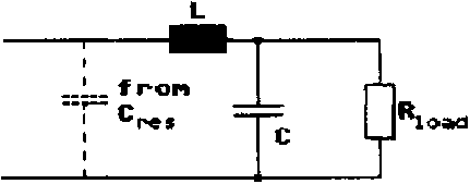
Method A requires something with a low resistance for dc and a high one for ac-components. Fitting therefore is obviously an inductor.
Method B requires something with a high resistance for dc and a low one for ac components. Fitting therefore is obviously a capacitance.
The best smoothing can be achieved, if both methods are used in the same smoothing circuit. Therefore in power supplies for very high quality you will find so called LC-smoothing circuits containing inductors and capacitors.
But inductors (often called “chockes”) are bulky, heavy and expensive. Therefore they are in most of the cases replaced by a resistor and form then together with the capacitor so called RC-smoothing circuits.
But resistors do not have an increased impedance for ac-components (compared with their resistance for dc).
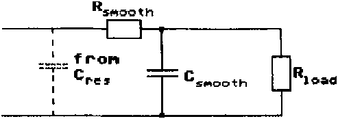
fig. 97
This fact makes the RC-smoothing circuits less effective than the LC ones - But in practice you will mostly find the RC ones.
CLOSER LOOK TO THE SMOOTHING FUNCTION OF A SMOOTHING CIRCUIT
1. Supposed the receiver represented here by the load resistor R
draws at 10 Volts a current of 30 mA. That means, the load resistor represents
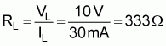
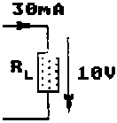
figure
2. Supposed resistor is 100 Ohms. Then the voltage drop across this resister will be:
VR1=R1 × IL = R1 × I = 30 mA × 100 W = 3V
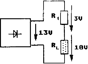
figure
Thus the supply voltage in this case must be = Vs = VR1 + VL = 3 V + 10 V = 13 V
3. Supposed the ripple-voltage across the reservoir capacitor of the powersupply is 2 Volts and assuming, a full-wave rectification.
That means a ripplefrequency of 100Hz. Supposed the reservoir capacitor has a capacity of 500 µF then its reactance is:
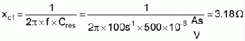
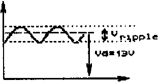
figure
The ripple voltage can be calculated according to the voltage division at Csmooth and Rsmooth
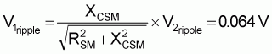

figure
Thus the ripple voltage has been reduced from 2V at the input to 0.064 V at the output of the smoothing circuit.
|
This means, it has been reduced for 97% |
10.5. STABILIZATION
10.5.1. GENERAL REMARKS
10.5.1.1. LOAD VARIATIONS
If the radio receiver produces much sound it will need more electric energy than if it will produce less sound. The voltage of the receiver has to be kept constant because of reasons we discussed already in former chapters. These differences in supply energy necessary for the receiver will therefore mean:
DIFFERENT AMOUNTS OF CURRENT DRAWN FROM THE SUPPLY.
10.5.1.2. INTERNAL RESISTANCE OF VOLTAGESOURCES
Every voltage source have a so called “internal resistance” which causes voltage drops at their terminals if any load current is drawn from the source.
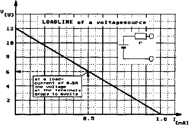
fig. 100
If the current is varied - (as shown above this is always the case with radio receivers) - therefore the voltage supplied at the terminals of the source will vary too (as shown in fig. 100)
10.5.1.3. PROBLEMS CAUSED BY THE SMOOTHING CIRCUIT
If you have a short look back to the last chapter, you can easily recognize, that with the common RC-smoothing circuit we have added to the internal resistance the Rv. With such a smoothing circuit we cause therefore an even stronger variation of the supply voltage. To overcome these difficulties we have to find now a possibility to STABILIZE the power-supply voltage.
10.5.5. METHODS OF STABILIZATION
Let us take as example the power supply which the output characteristics plotted in fig. 100.
It is intended to use it for a receiver operated with 6 Volts.
The maximum current to be delivered by this supply at 6 Volts is 500 mA.
If the receiver uses a maximum current of 500 mA this supply is OK. As we know, the receiver will draw different currents - which means: the voltage would increase up to 12 V.
10.5.5.1. PARALLEL-STABILIZATION
Here the overall current drawn from the supply will be kept constant by a component giving way for a current in a second path as soon as the voltage tends to increase above 6 V.
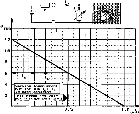
fig. 102
PARALLEL CONTROL STABILIZING CIRCUIT USING A ZENERDIODE EXCLUSIVELY
the most simple circuit to achieve the parallel stabilization is to connect a so called ZENERDIODE in parallel to the load.
FUNCTION:
Let us first have a closer look to the characteristics of a zenerdiode. The characteristics of one called B6Z2 is shown in fig. 105. It is easy to see, that the zenerdiode has a very flat characteristics first (which means a very high resistance) and from a special point on it has an extremly steep-characteristics (which means a very low resistance).

fig. 105
The working points between which the diode is useful for stabilization are found at the borders of delta-V.
Taking the second part of the characteristics for a moment theoretically totally vertical, the zenerdiode looks like a contact closed as soon as the voltage at its terminals is exceeding a special limit (the zenervoltage).
Even though this is only a theoretical view, it shows us what the zenerdiode is going to do in the simple stabilization circuit: It will let flow a big amount of-current as soon as the zenervoltage is exceeded.
That means too: the voltage at its terminals is changing only very slightly while the current changes tremendously - as seen in fig. 105 fig. 106 shows this rather simple circuit containing a Zenerdiode, which is able to do the job rather well.
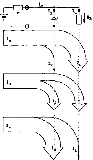
fig. 106
The overall current flowing in the circuit is kept constant here by the zenerdiode.
The next chapter will show us by graphical means how this is working by using the characteristics of the zenerdiode.
GRAPHICAL DERIVATION OF THE FUNCTION OF A SIMPLE PARALLEL CONTROLLED STABILIZATION.
fig. 107 shows the typical graph of a Zenerdiode connected in series to a resister (here the internal resistor of the voltage source or even a special series resistor)
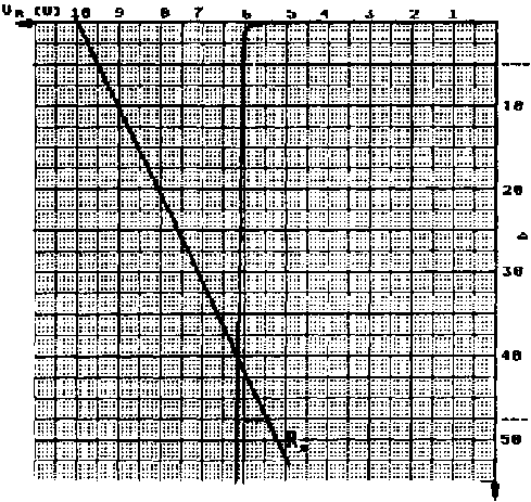
fig. 107
If there is a load-resistance lower than infinite it can be represented by one of the graphs shown in fig. 108.
fig. 108
As we know, the graph is as steeper as lower the resistance represented is. If both components - Rload and the zenerdiode - are connected in parallel, there are passing two currents through them in parallel. If we want to know the overall current flowing through both components, we can find that easily, by constructing the overall characteristics, of both, by adding the vertical represented currents.
fig. 109
fig. 110
The characteristic obtained by that method is shown in fig. 109. is the overall-characteristics of zenerdiode and loadresistor in parallel.
fig. 109
If we return now the characteristics of the internal resistor back to our field, we can easily read from it, how much voltage will be found at different load resistors.
Homework;
By using fig. 110 find out, what the voltages at the load are, with the different loadresistance.
Find out what voltage would appear with the same voltage source and the given load resistors, without a stabilizing circuit. Plot the stabilized and the unstabilized voltage over the load currents.
figure
10.5.2.2. SERIES STABILIZATION
Here the voltage appearing at the terminals of the voltage source is divided in one part dropped at the load (the receiver) and a second part connected in series dropping the rest of the voltage not to be allowed at the receiver.
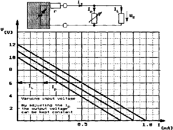
fig.
104
|
| |||||||||||||||||||||||||||||||||||||||||||||||||||||||||||||||
Radio and Electronics (DED Philippinen, 66 p.)
11. ACTIVE COMPONENTS -2- / TRANSISTORS
11.1. CONSTRUCTION OF A TRANSISTOR
Transistors consist of three sections of a semiconducting base material. The two outer sections being doped in opposite sense, the centre section - called the BASE. The outer two sections are called:
COLLECTOR and EMITTER.
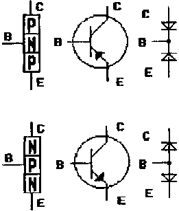
fig. 119
Between these three sections and obviously between the three terminals too, there are two junctions of PN-type, these two junctions can be looked at as two diodes connected in opposite direction.
Connection basically:
If the transistor is used in an electronic circuit generally the collector-base junction is connected in reverse direction and the base-emitter junction is connected in forward direction.
Function (simplified):
If there flows a considerable small current through the base-emitter junction, this allows a considerable strong current to flow from collector to emitter. The sketch in fig. 122 shows this behaviour very simplified.
fig. 122a

fig. 122b
Notation of transistors:
To find out which type of transistors we deal with we have to know the notation of transistors.
In most cases you find a combination of letters and figures on the case of the transistor. To find out exactly the specifications of this very transistor. You have actually to use a databook.
But very often the notation gives us hints about what the transistor is normally used for.
How does the transistor do its job?
Incidental remark:
Here will be derived the function of an NPN-transistor and an PNP-transistor in a similar manner.
It must be kept in mind, that the base layer in any transistor is very tiny in comparison with the two other layers. To explain the function of a transistor it must be dealt with as being connected to voltage sources. There are different possibilities to connect it two voltage sources. The possibility used here is the so called COMMON EMITTER CONNECTION.
This connection is the most often used one in practice. Therefore the other connections will not be dealt with here.
By the way: the transistor technology is still developing and this development led to new transistors, which can be used in common-emitter connection even in cases where in former times another connection was necessary.
Derivation of the function:
1. If a transistor is connected to a voltage-source as shown in fig. 123 it will not conduct any current, because one of the PN-junctions is always biased in reverse direction.
fig. 1232. As long as the voltage between base and emitter is connected in reverse direction there will not flow any current as well - as we know already from our explanations about a diode.
fig. 1243. As soon as a voltage source is connected to the base-emitter junction in forward direction, and the voltage reaches a level higher than the so-called threshold voltage, of this junction, there will start to flow a current through this junction.
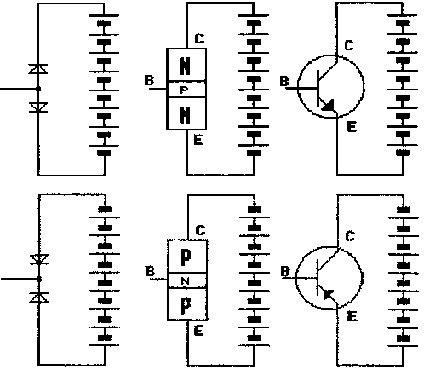
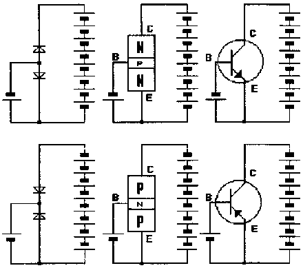
This current causes within the transistor a very special effect:
The chargecarriers (electrons or “holes”) enter the base-region. But as the base region is very narrow, these chargecarriers comming in big numbers from the wide emitter-region cannot be channelled totally through the base terminal.
So they invade the depletion-layer of the collector-base junction. But at the collector terminal with a strong polarity of the voltage-source connected to the collector and the emitter-terminals waiting for those charge-carriers, and attracts them through the depletion layer causing a current to flow through a PN-juncion (collector-base junction) in reverse direction.
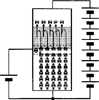
fig. 126
The current channeled from collector to emitter (or vice versa) by the base current is called the COLLECTOR CURRENT.
This collector current is depending on the amount of BASE-CURRENT which was the origin of the effect.
As soon as the base current will be changed or interrupted, the collector current will change proportionally or will be interrupted as well.
The big advantage of the transistor is: the collector current is between 20 to 200 times bigger than the base - current.
SUMMING UP:
The transistor is a device which makes it possible to control.
A big current (COLLECTOR CURRENT) by a very small current (BASE CURRENT).
11.2. CHARACTERISTICS OF TRANSISTORS
If a technician wants to use transistor in a certain electronic device, he has to know first exactly how it will work under the conditions given in this very circuit. To make it possible to predict the function of such a transistor, the producers of transistors supply the users with so called “data sheets”.
Beside a lot of values given directly in those data sheets, they are also plotting the most important characteristics of the transistors.
FIELD OF CHARACTERISTICS
If we consider for a moment again our transistor we find our easily that there are four electrical factors on which it is depending on.
|
- the base-emitter voltage |
VBE |
|
- the base-current |
IB |
|
- the collector-emitter voltage |
VCE, and |
|
- the collector-current |
IC |
To make the relations between those factors more obvious, we find nowadays very often the so called
FOUR-QUADRANT-FIELD
Fig. 130 shows a plot of such a kind.
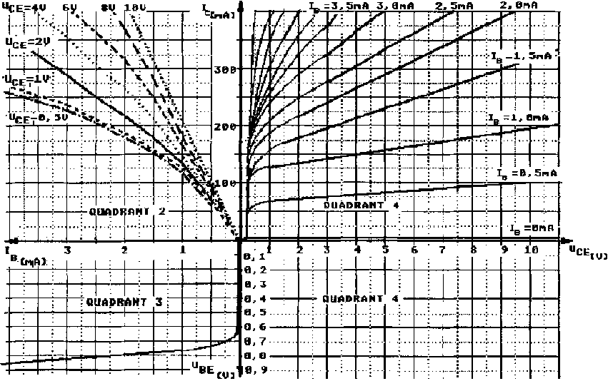
fig. 130
The four quadrants are called:
QUADRANT 3 - shows the relation between the base-current and the base-emitter voltage. This is always a graph very similar as the graph of a diode, only turned around, so that it fits into this part of the field. So the base and the emitter are connected to the input of the common-emitter-connection, the characteristics is called the INPUT-CHARACTERISTICS.This term can be understood too if you think about the explanation of the function of a transistor, where the base current was described as the precondition for the collector current.
QUADRANT 1 - shows the relation of the collector-current and the collector-emitter-voltage. We can see it also as the representation of the resistance between collector and emitter. So this resistance is depending on the base current, there are different graphs, for different amounts of base-current. Because the collector and the emitter are connected to the output side of a common-emitter connection, the characterics shown in this quadrant are called OUTPUT-CHARACTERISTICS.
QUADRANT 2 - represents the relation between the collector-current and the base-current. This means, it shows the relation between one factor which is part of the input side of the circuit and another which is part of the output side. Therefore this graph is called the MUTUAL-CHARACTERISTICS.
QUADRANT 4 - is used very rarely and only its name shall be only mentioned here: FEEDBACK CHARACTERISTICS-
11.2.1 HANDLING OF CHARACTERISTICS OF TRANSISTORS
11.2.1.1. CONSTRUCTION OF THE STATIC-MUTUAL-CHARACTERISTICS
Even if you find in a given four-quadrant-characteristics a so called mutual-characteristics this is very often not fitting, because this characteristics is changing when collecter-emitter-voltage is changing. For this reason it is necessary to know how this characteristics can be found for each voltage you want it.
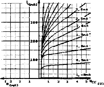
fig. 131a
A) draw a vertical line into the 1. quadrant at the collector-emitter-voltage for which you want the mutual-characteristics.
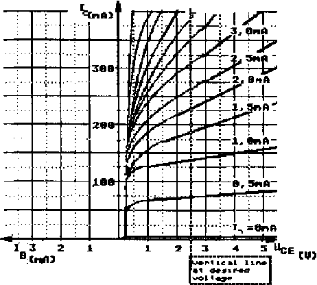
fig. 131b
B) draw horizontal lines through the points at which this vertical line is crossed over by the lines of the output-characteristics.
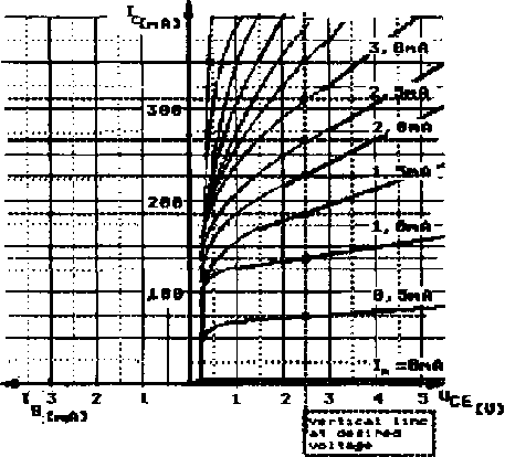
fig. 131c
C) Find out the values of the base current represented by the crossed over lines in the output-characteristics and mark the horizontal lines at those values of the base-current in the 2. quadrant.
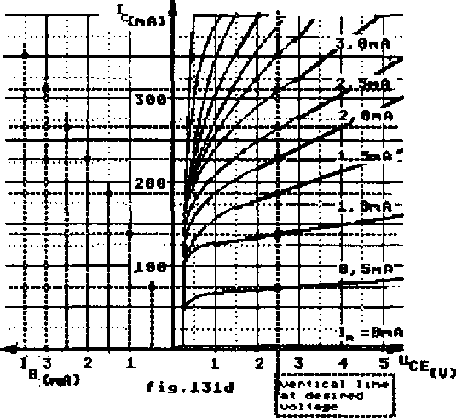
fig. 131d
D) Connect all the points which you have found to get a new graph - this is the mutual characteristics for the desired collector-emitter-voltage.
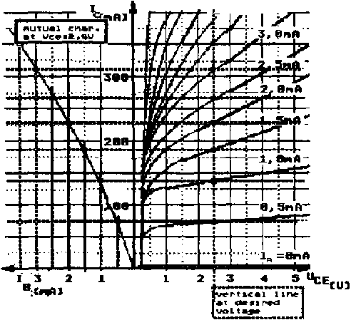
fig.
131e
11.2.1.2. CONSTRUCTION OF THE DYNAMIC MUTUAL CHARACTERISTICS
If the transistor is connected in a circuit the mutual characteristics changes according to the parameters given in this very circuit. The graph, showing this characteristics, is called the DYNAMIC MUTUAL CHARACTERISTICS and it shows actually the ability of amplifications of this very circuit.
To construct it, we enter the loadline of the collector-resistor into the output quadrant and find the values of the collector-current for each given base-current. The relation Ic/Ib is represented then in the 2. quadrant as shown in fig. 133.
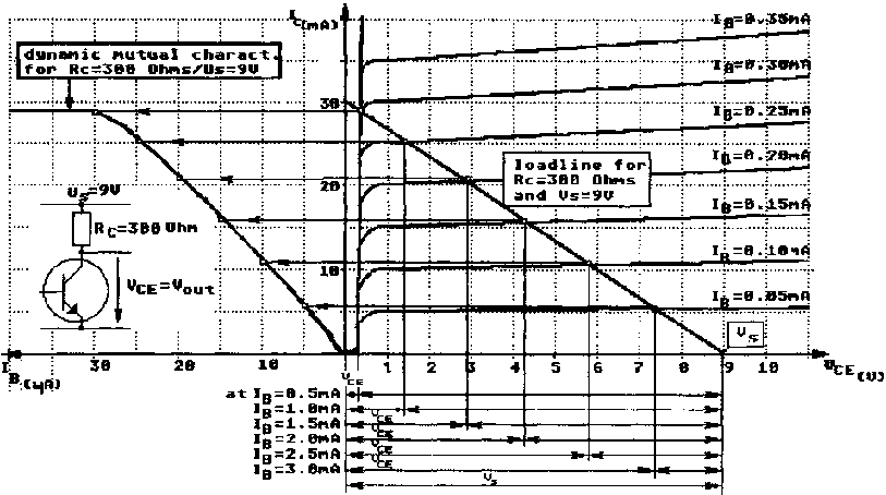
fig. 133
For the given circuit of a transistor with the given characteristics, an Rc of 300 Ohms and a supply voltage of 9 Volts, we find that the amplification is rather constant as long as the base-current does not exceed 3 mA. Above this value the amplification is decreased down to 0.
Mind too, that the output voltage Vce is high at low base-currents (low-input-signal) and vice versa.
11.2.1.3. CONSTRUCTION OF THE MAXIMUM-POWER-LINE
Each transistor has a maximum power rating. Which means: this is the power which can be dissipated by it, without danger of destruction.
Therefore it is extremly important to make sure that the transistor is always operated on “the safe side” - which means in our field of characteristics: on the safe side of the maximum power line. For this reason it is necessary to be able to construct the maximum-power-line.
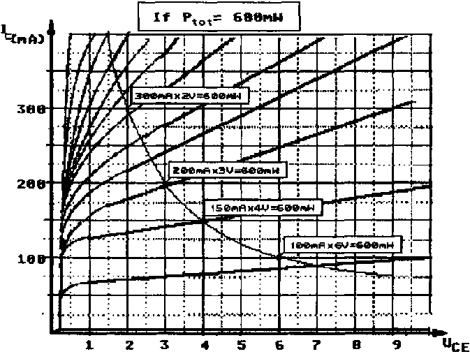
fig. 132
A) find in the data sheets the maximum permissible power for the transistor.
B) Calculate for various collector-emitter-voltages the permissible collector-current for this power. (The power dissipated for the input-values is so minute, that it can be neglected).
Ic = Ptot / Vce
C) Construct the Power-line by inserting the values of Ic for the different collector-emitter voltages.
The maximum powerline represents the field of application in a safe-area and a not allowed area.

fig.
132a
|
| |||||||||||||||||||||||||||||||||||||||||||||||||
Radio and Electronics (DED Philippinen, 66 p.)
12. AMPLIFIERS
Amplifiers have to “amplify” signals. This means an input signal with a relatively low energy (low current and low voltage) is enlarged to an output signal of much more energy and a shape which should be (ideally) the same like the input-signal. Fig. 138 shows the general symbol of an amplifier.
fig. 138
An amplifier works on the following PRINCIPLE:
Beside the input-signal the amplifier is supplied with a supply voltage and a supply current, which means a supply power. This supply power is many times higher than the input signal power. Control-components (like for example transistors or triode valves) convert a more or less high percentage of the power into an output-signal. The part of the supply-power converted into the output signal is called the useful power Pout of the amplifer, while the rest of the supply power is dissipated as losses.
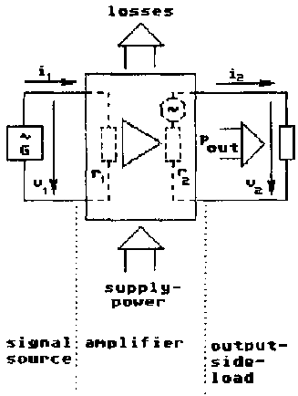
fig. 139
The main characteristics, which make an amplifer a good or a less good one, are the following:
A) a big difference between signal-power and NOISE-POWER. Every electrical device is producing electrical oscillations while operated.These oscillations should be kept extremly small in comparison with the inputsignal.
B) As less DISTORTION of the shape of the input-signal as possible. (Low distortion or “Klirr-factor”.)
C) A good matching (see chapter - MATCHING) between:
- the input of signal source and the in put resistance and
- the output resistance and the load.
D) The fitting BANDWIDTH and a good FREQUENCY RESPONSE which means constant amplification over the whole range of frequencies which the amplifier is due to amplify.E) A good EFFICIENCY which means as less losses as possible.
F) A good WORKING CONSTANCY which means all characteristics should be as constant as possible even under conditions when the temperature of the amplifier and the supply voltage is varying.
Amplifiers can be differentiated either by the special tasks they are built for, like for example:
- Preamplifiers (low level amplifier)
- Power-amplifiers
- NF-HF amplifiers
- selective amplifiers, or
- wide-band amplifiers....
Or by the principles they are working on, like for example:
- class A amplifiers
- class B amplifiers, or
- class C amplifiers.
12.1. STRUCTURE OF A CLASS A AMPLIFIER
INTRODUCTION
Let us suppose the amplifier we are looking at has to amplify a sinusoidal signal as shown in fig. 140.
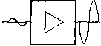
fig. 140
Applying our knowledge about transistors you probably would come to suggest a circuit similar like shown in fig. 141. where a tiny signal source supplies a base-emitter-junction and the big collector-current is originated from the power-supply. Here is mentioned a NPN-transistor, but the principle is exactly the same with a PNP-transistor.

fig. 141
WHAT IS THE COLLECTOR RESISTOR NECESSARY FOR?
The circuit shown in fig. 141 would be in the theoretical sense of the word already an amplifier.
But the sinusoidal current flowing here in the so called collector-circuit, is not useful anywhere.
Neither is it operating anything (like a loudspeaker) nor is it producing a signal at the output which could be transmitted to another amplifier stage.
This is the reason why we find in all amplifiers at the output either a component which will use the signal current itself or at least cause a voltage drop. This part of the amplifier is called the collector resistor Rc, as shown in fig. 142a.
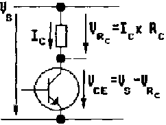
fig. 142a
If there is flowing now a collector current Ic it will cause a proportional voltage-drop at this collector resistor.
WHAT IS THE POINT OF “QUIESCENCE”.
Referring to the example in the last chapter we can easily state that:
VRC = VS - VCE
With the formula in the last chapter we can now derive that the voltage VRC can vary between the two extreme values.
1. Ic = 0 then VRc = 0
2. Ic = Maximum VRc = Vs
(whereby IC maximum = VS/RC)
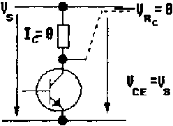
fig. 142b
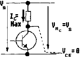
fig. 142c
At the output of the amplifier, we want to find an exact sinusoidal signal of exactly the same frequency again. This can only be achieved if the output-voltage can oscillate, which means: it must be free to increase and to decrease, from the level which it has at an input-voltage of 0 Volts - a status which will be called from now on:
QUIESCENCE. BIASING WHAT FOR?
If the input-signal would be directly connected to the base of our amplifier transistor as shown in fig. 142d we would find only a change of the output voltage during the period between point 1 and 2 as long as the input signal is above 0.6 Volts. This would not be fitting to the precondition developed for a class A amplifier in the last chapter.
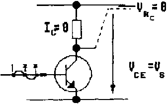
fig. 142d
To set the output to the so called quiescent-voltage we have to make sure that at quiescence at the input, there is already flowing a collector-current which must be about half of the maximum collector current, therefore we have to let flow an input-current (base-current) even if there is not yet any input-signal.
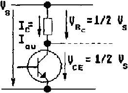
fig. 142e
We call this method BIASING our amplifier circuit. The simplest circuit to achieve this is shown in fig. 143. Here a base-current is allowed to flow which is big enough to keep a collector current flowing which is half of its maximum. But if you have a short look back to the input-characteristics of a transistor, you can easily see, that a tiny change of the input voltage would cause a tremendous change in base-current, which would cause again a tremendous change of collector-current, and therefore too a tremendous change of the output-voltage. This means, that the quiescence-voltage is not stabil. As will be seen later, this would have very big disadvantages for the working of our amplifier.
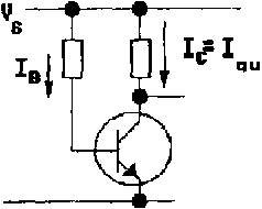
fig. 143
To reduce this problem, it is prefered to bias with voltage-dividers like shown in fig. 144.
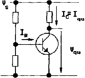
fig. 144
REPRESENTATION OF THE QUIESCENT-POINT IN A FOUR-QUADRANT-CHARACTERISTICS OF THE AMPLIFIER TRANSISTOR.
We can find the so called quiescence-point as well in our four-quadrant-characteristics.
Therefore we have to enter into the first quadrant the loadline of the collector-resistor. The transistor should have the characteristics given in fig. 143. The quiescent-voltage should be in this case about 4.5 Volts.
To achieve this, we have to supply the transistor with a base-current of about 0.14 mA. And therefore we need a base-emitter-voltage of 0.75 V. As you see in fig. 144a.
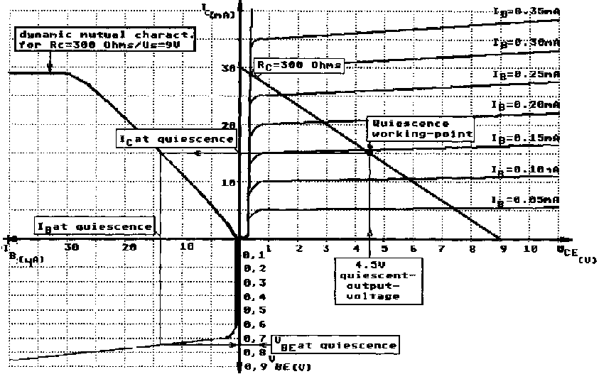
fig. 144a
HOW TO INJECT NOW THE INPUT SIGNAL TO SUCH A AMPLIFIER CIRCUIT?
If we could connect a signal-source directly to the input-terminals of the amplifier as shown in fig. 144 the signal-source would pass a dc-current through the lower resistor.
But the signal-source is always a very weak energy-source. So by such a dc-current the signal could be distorted very heavily. The problem can be solved by the following idea:
We know, the input-signal, is always an ac-voltage (at least in radio-technology). Therefore we have to make sure that only an ac-current is allowed to enter the input terminals of the amplifier-circuit.
As you know from chapter 8.2 the capacitor is the component which we need here.
If we connect such a capacitor in series there can only flow an ac-current through the inputcircuit.
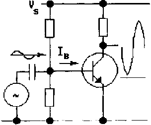
fig. 145
HOW TO GET THE SIGNAL OUT OF THE STAGE?
As long as the amplifier is not the last one in a row of stages, its signal has to be entered to another stage.
The next stage will be constructed similar like the stage we came to know just now.
If we would connect another stage directly without a capacitor between the stages, there would again flow a dc current from one stage to the other, and this would mean again distortion.
Therefore: at the output we will find another capacitor. Between two stages, very often the input-capacitor is at the same time the output-capacitor. Both capacitors are called: COUPLING CAPACITORS.
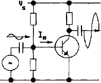
fig.
146
12.2. FUNCTION OF A SIMPLE CLASS A AMPLIFIER
We know now the basical components of a class A amplifier and it is possible to have a closer look to the effects in this circuit when a signal is injected to the input of the circuit of fig. 147 (page 43).
- Suppose the signalsource has a positive halfwave of a signal between time 1 (t1) and time 2 (t2). This will cause a charging current for C1.- This charge-current is flowing via the loop: signalsource, C1 and R2. At R2 this current will flow additional to the current flowing at quiescence. This means too an increase of the voltage at R2.
- The voltage at R2 is equal to the base-emitter-voltage. An increase of that voltage causes (according to the input-characteristics of the transistor) an increase of the base-current.
- The output-characteristics of the transistor tells us, that an increase of base-current causes an increase of collector-current.
An increase of collector-current lets the voltage at the collector-resistor increase, which again causes the collecter-emitter-voltage to decrease.
-Now there will flow a discharge current through C2 and this will cause a negative voltage drop at the load-resistance.
- Between t2 and t3 the negative halfwave will be injected, this will cause the same effects in our circuit, but with opposite direction.
fig. 147
REPRESENTATION OF THE FUNCTION OF A CLASS A AMPLIFIER IN THE FOUR-QUADRANT - CHARACTERISTICS.
Supposed the circuit is the same as described for fig. 147, and supposed that the input-signal has an amplitude of 50 mV we would find an output signal as derived in fig. 147a.
fig.
147a
12.3. ADVANCED CLASS A AMPLIFIER
PROBLEMS, IN A SIMPLE CLASS A AMPLIFIER.
If amplifiers would be constructed like shown in fig. 147 they would only work correctly for a very short time.
After a short while of operation they would get “instabil” and would produce a lot of distortion.
DISTORTION means: the shape of the output-signal is very different from the shape of the input-signal.
DISTORTION DUE TO A WRONG “QUIESCENT-VOLTAGE”
The output-voltage V2 can only reach levels between full supply-voltage and almost 0 Volts.
EFFECT OF TOO LOW BIASING VOLTAGE
Let us imagine the amplifier is supplied with maximum input-voltage V1, so that the sinewave - produced at the output - has a peak-to-peak-voltage of almost full supply-voltage as shown in fig. 147a.
If the quiescent voltage is now shifted because of any reason towards lower values the output voltage never can be higher than the supply-voltage. This means: during the negative halfwave of the input signal the output signal would be distored, as shown in fig. 148a.
figure
EFFECT OF TOO HIGH BIASING VOLTAGE
the same problem arises if the quiescent-voltage at the input increases. Now the output signal would be destorted during the positive halfwave of the input signal as shown fig. 148b.
fig. 148a
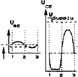
figure

fig. 148b
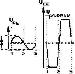
figure
EFFECT OF A TOO HIGH AMPLITUDE OF THE INPUT SIGNAL THE
In case, the quiescent-voltage is constant but the input-signal is bigger than allowed for this amplifier-stage. This would cause a distortion on both peaks of the output-signal as shown in fig. 148c.
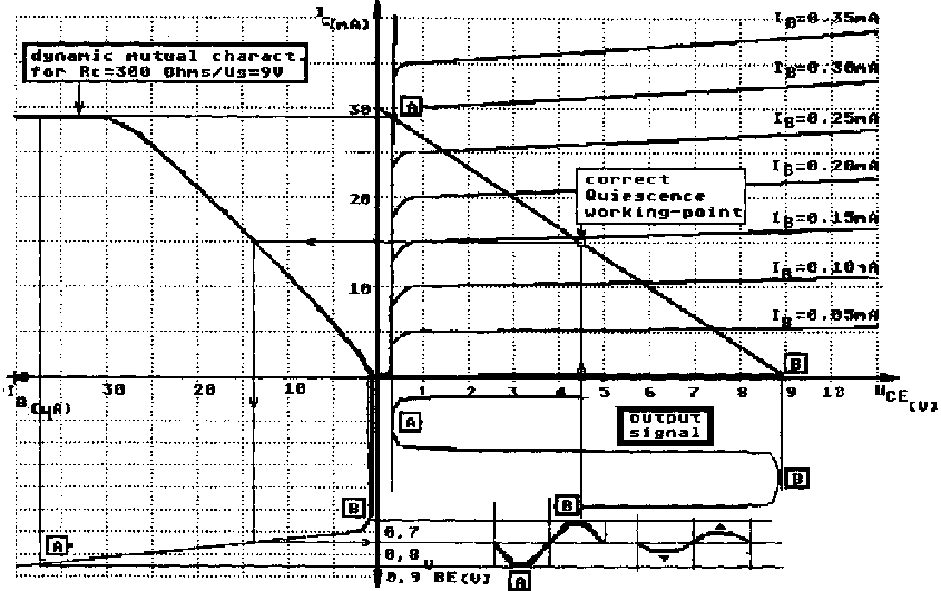
fig. 148c
The method how to limit the input-signal will be shown later. At this stage of our course it is necessary to understand how the quiescent-voltage can be hold constant.
12.4. STABILIZATION OF THE QUIESCENT VOLTAGE
As explained in chapter 9.1. the transistor is a component, which is very sensitive to increasing temperatures.
It is a semiconducting component, and therefore with growing temperature its resistance is decreasing.
In case of our transistor in an amplifier-stage, the relatively high collector-current causes a rise in temperature. This increase of temperature causes a bigger conductivity in the transistor. Bigger conductivity lets rise the collector-current (even though the base-current is still the same). Even if this process is a slow one, the increase of collector-current, causes a decrease of output-voltage at quiescence, and therefore a drifting quiescence-voltage.
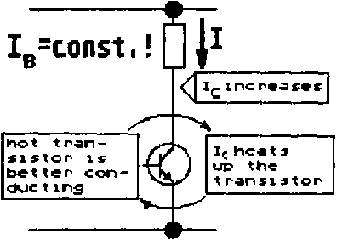
fig. 149
There are several methods, how to diminish this effect:
EXAMPLE A:
By tapping the biasing path from the collector-current.
Function:
If the collector-current increases because of increased transistor temperature the collector current increases and the voltage across the voltage divider will tend drop as well. So the base-emitter-voltage will drop too - which lets decrease the base-current and therefore the original increase of the collector-current will be cancelled.

fig. 150 - A
EXAMPLE B:
By a so called EMITTER-RESISTOR. This resistor is dimensioned in order to drop about 10% of the supply-voltage ant quiescence.
Function:
If the collector-current at quiescence tends to increase the voltage at the emitter-resistor tends to increase as well. So base-emitter-voltage is the difference of the voltage across the lower biasing resistor and the voltage across the emitter resistor, the base-emitter-voltage tends to drop then as well. Dropping base-emitter-voltage causes a decreasing base-current and this causes the collector-current to decrease as well.
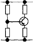
fig. 150 - B
So the original increase of collector-current will be cancelled.
WHAT FOR THE EMITTER-CAPACITOR THEN?
The emitter-resistor has - beside its stabilizing effect - a big disadvantage as. The input-currents and the output-currents have to pass it. And this causes a voltage drop for input and output-values.
So, by an emitter-resistor exclusively the amplifier-stage would loose a lot of its efficiency. The solution can be found by the following thoughts:
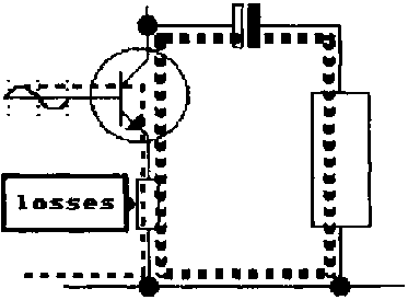
fig. 151a
Input- and output-currents are ac-currents while the distorting effect of the increasing collector-current is a dc-component. So we have to bypass the ac-components. As we know a capacitor lets pass again ac- but not dc-values. So the currents - bypassed - are rather high here, the capacitor must be rather big (very often it is an electrolyte-type).
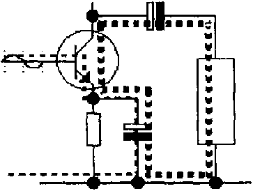
fig. 151b
NOW WE KNOW HOW A NORMAL SO CALLED CLASS A AMPLIFIER IS MADE UP.
WHERE ARE CLASS A AMPLIFIERS USED?
Always if the outputpower of the amplifierstage is low. This means, we will find this amplifier class for example in IF-stages, RF-stages and audio-preamplifiers.
HOMEWORK:
1. Label all the components in the circuit.
2. State which voltages you should measure (roughly) at this amplifierstage at quiescence.
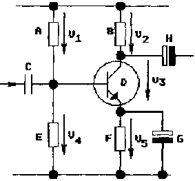
fig. 152
A:...........................................
B:...........................................
C:...........................................
D:...........................................
E:...........................................
F:...........................................
G:...........................................
H:...........................................
V1:..........................................
V2:..........................................
V3:..........................................
V4:..........................................
V5:..........................................
|
| ||||||||||||||||||||||||||||||||||||||||||
Radio and Electronics (DED Philippinen, 66 p.)
13. CLASS B AMPLIFIERS
13.1. LIMITS OF CLASS A AMPLIFIERS
In very cheap and small transistorradios we find sometimes - as an exception - class A amplifier even for the power stage, but operating only an earphone or a very tiny loudspeaker. The reason why is easy to see if we have a closer look to the quiescent point.
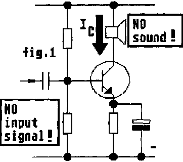
fig. 153
If you have a short look back to fig. 144a you will easily see, that in this case in a class A amplifier the output-voltage must be half of the supply voltage. The collector-current is therefore half of the maximum current and this means: AT QUIESCENCE (NO INPUT SIGNAL AND NO OUTPUT SIGNAL) THE POWER CONSUMPTION OF A CLASS A AMPLIFIER IS ALREADY 25 % OF THE MAXIMUM POWER CONSUMPTION OF THIS STAGE.
This makes clear: for high amplification of considerable power another kind of amplifier is necessary otherwise the energy losses are too much.
The next amplifier class which we will come to know now is called class B amplifier and it is designed for power-amplification.
A difference between class A and class B amplifiers easily to be realized is:
- Class A amplifiers amplify with a single transistor a whole sinewave of the input signal.
- Class B need at least two transistors to do the same.
GENERALLY:
If we want to avoid the losses - caused in a class A amplifier at quiescence - we have to shift the quiescence working point to lower powers.
This can be achieved by reducing the base-current to about “0”.
But if the base-current is kept “0” at quiescence at the output of a COMMON-EMITTER-CONNECTION (as we call the transistor circuit used up to here) can only be produced half of a sine-wave as shown in fig. 154.
fig. 154
So we have to use two transistors in order to amplify both parts of the sinewave and to find a way how to “couple” both parts together again.
13.2. CLASS B AMPLIFIERS WITH TRANSFORMERS
In power amplifiers of older types of receivers we find often circuits which are called PUSH-PULL-AMPLIFIERS. In this kind of an amplifier one transistor amplifies only one half of the input signal wave, the other half of the signal is amplified by another transistor.
One circuit which has been commonly used in such push-pull amplifiers is shown in fig. 162. It has two transistors and two centre-tapped transformers.
T1 has a centre-tapped secondary coil and it is used to split the input signal into two halfwaves, and to feed the bases of the two transistors alternatively.
T2 has a centre tapped primary winding and is used to combine again the two amplified halfwaves of the output-signal.
fig. 162
Transistor V1 is part of an PREAMPLIFIER. It controls the collector-current of V1 through coil “a” of T1. If this collector current increases, there will be a voltage induced at the secondary coil “b” of T1. This has here a downward direction, so we find now at the base-emitter-junction of V2 a voltage which is directed forward while at V3 it has a reverse-direction. ® V2 will be conducting and ® there will flow a collector current through V2 and the part 1 of coil “b” of T2. This induces a voltage in the secondary coil of T2 and a current through the loudspeaker.

fig 162b
If this collector current through V1 decreases, there is a voltage induced at the secondary coil “b” of T1. This has here a upward direction, so we find now at the base-emitter-junction of V3 a voltage which is directed forward while at V2 it has a reverse-direction ® V3 will be conducting and ® there will flow a collector current through V2 and the part 2 of coil “b” of T2. This induces an opposite voltage in the secondary coil of T2 and an opposite current through the loudspeaker.

fig. 162a
The two resistors R1 and R2 are necessary to avoid a distortion which would be caused if there would be no biasing of the two bases of transistors 2 and transistor 3. As demonstrated in fig. 155 without biasing the start of the output halfwave is delayed till the input signal has passed the level of the so called THRESHOLD VOLTAGE of about 0.6. Volts.

fig. 155
This kind of push-pull-amplifier was used a rather long time, but it is almost no more found in modern transistor radios because of the bulkiness and the high price of transformers. These disadvantages have been the cause for a change in technology of power amplifiers nowadays.
13.3. CLASS B AMPLIFIERS WITHOUT TRANSFORMERS
The intention was to get rid of the transformers which had been used to “split” the input signals into two halfwaves. Without transformers we cannot “turn around” one half of the input signal. So it is necessary to let the current flow in both directions. This is not possible with transistors of the same type.
We have to use a combination of an NPN and a PNP transistor. They must be very similar in characteristics and therefore they are called to be complimentary.
13.4. POWER AMPLIFIER WITH COMPLIMENTARY TRANSISTORS.
The following drawings show how a complimentary push-pull amplifier is working.
fig. 163
Fig. 163 shows two circuits. The upper one with a NPN transistor will have current through R1 while there is a positive signal at the input. The lower circuit will have current through R2 always when there is a negative input signal.
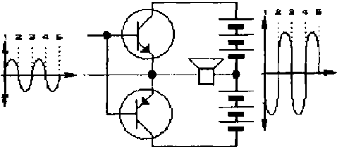
fig. 164
Fig. 164 shows the two circuits of fig. 163 combined. Now the two resistors are replaced by a single loudspeaker. Both currents - explained in fig. 163 - flow through the loudspeaker so causing an ac-current in the loudspeaker. This fits to our desire, to have a current flowing only if there is a signal voltage different from quiescence.
The big disadvantage of the circuit in fig. 164 is, that there are two batteries necessary for it.
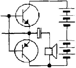
fig. 165
Fig. 165 shows a circuit which gets rid of that disadvantage.
If there is a positive input signal, there will flow a current via the NPN transistor, the capacitor will have a capacity big enough so that it can be charged completely only during the longest possible half-waves (at lowest frequencies).
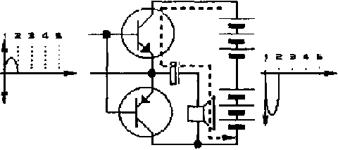
fig. 166a

fig. 166b
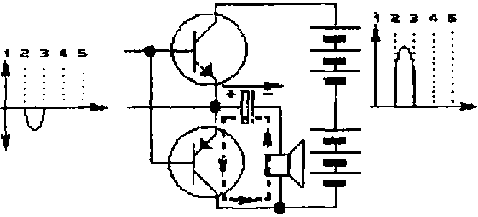
fig. 166c
So we will find after the positive halfwave at the capacitor a full positive charge as shown in fig. 166b. With a negative input signal the PNP-transistor gets conducting and there will flow a current - originated from the capacitor as a voltage-source - through the PNP-transistor and the loudspeaker as shown in fig. 166c.
The current flowing now through the loudspeaker is flowing backward - which means: there is flowing an ac-current through the loudspeaker.
Improvements of the simple circuit of a complimentary push-pull amplifier.
The circuit derived in fig. 166 has still two main problems which must be solved before it can be used for a receiver.
PROBLEM 1:
It is easy to see, that the voltage at the base of Tr1 can never reach a value higher than that of the supply voltage. But supposed Tr1 is made conducting (by a relatively high base-current) then the voltage at the emitter of Tr1 has a potential which is just 0.2 Volts lower than the supply-voltage.

fig. 167
As we know: to inject a base-current to Tr1 we need at least 0.7 V between Base and Emitter of Tr1.
This shows: With circuit shown in fig. 167 it will never be possible to make Tr1 fully conducting.
Consequence:
We have to find a method to supply point A with a potential about 0.6 V higher than the supply voltage. One possibility to achieve this is shown in fig. 168. But this is a very complicated and inconvenient way, because we need an additional cell for it.
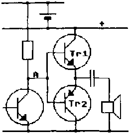
fig. 168
Practical solution:
The most common way of solving that problem is the so called BOOTSTRAP CAPACITOR C2 shown in fig. 169.

fig. 169
Its function is like that: At “NO” input signal the voltage at point A will be about half of the supply voltage because there is flowing a medium current. The voltage at point C through the two collector resistors of Tr.3 will be about 75 % of the supply voltage. If now a negative signal occurs at the input the voltag at point A will be raised. Of course the voltage at point B is increased as well (base-emitter-voltage at Tr1 maximum 0.6 V). So C2 has a rather big capacity the voltage at point C reaches values higher than the full supply voltage.
PROBLEM 2:
If the bases of Tr.1 and Tr.2 are connected like shown in fig. 170 we would face a so called CROSSOVER-DISTORTION as shown in fig. 170 because it takes always at least 0.7V of voltage change until the transistors are starting to get conducting. A first solution would be to insert a resistor R2 as shown in fig. 171. But the dimensioning of R2 is extremly sensitive because:
- if it is too small there will be still a crossover distortion, and
- if it is too big there will be a lot of losses or even a short circuiting through Tr.1 and Tr.2
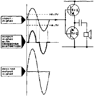
fig. 170
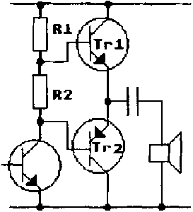
fig. 171
A better solution is to fit in two diodes like shown in fig. 172. In order to have an automatic adjustment in case of heating up of the transistors, very often is used an additional thermistor connected in parallel to the diodes as shown in fig. 163. This thermistor is mostly fixed to the heat sink of the transistor.
So transistors heat up, the thermistor which will cause a drop of its resistance and therefore a voltage-drop across the two diodes. This again causes a decreasing base-current for both transistors Tr.1 and Tr.2.
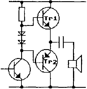
fig. 172
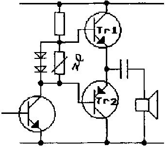
fig. 173
In order to avoid lude a crossover-distortion as far as possible, in practical circuits we find at last an adjustable resistor connected in series to our diodes. This adjustable resistor is used to preset the voltage across the two bases exactly to a condition where at quiescence a small collector current just starts to flow.
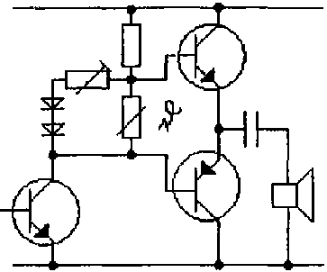
fig. 175
A rather advanced power amplifier of the COMPLIMENTARY PUSH PULL TYPE is shown in fig. 176.
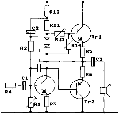
fig. 176
CHECK YOURSELF:
1. Explain how a Push-Pull amplifier with transformers is working.
2. Explain how a complimentary Push-Pull amplifier is working.
3. Explain what each component in fig. 176 is useful for.
|
| ||||||||||||||||||||||||||||||||||||||||||||||||||||||||||||||||||||||||||||||||||||||||||||||||||||||||||||||||||||||||||||||||||||||||||||||||||||||||||||||||||||||||||||||||||||||
14. DETECTOR OR DEMODULATOR
So we deal within this course only with AM-receivers we will of course deal her only with AM-Demodulators. But we should bear in mind, that there are so called FM-detectors too, which are very different from AM-detectors.
2. Function of the detector
The detector has to filter the AF-signal from the RF-signal (in a “TRF-receiver”) or the IF-signal (in a superhetreceiver).
If we remember the IF-signal as shown in fig. 180 (upper part) we see easily that the detector should produce the signal which is represented by the intermitted line.
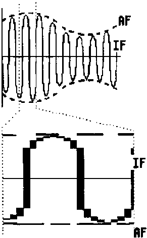
fig. 180
The way how a detector is working can easily be understood if we at first concentrate on a short interval of the IF-signal shown in fig. 180. (lower part).
Within the time interval represented here the intermitted line is almost horizontally, which means: the AF-signal desired at the detector output is equal to the peak voltage of the IF-signal. This could be produced by just rectifying the IF-signal and smoothing it by a reservoir-capacitor. But doing this would lead to an output signal as shown in fig. 181. (upper part).
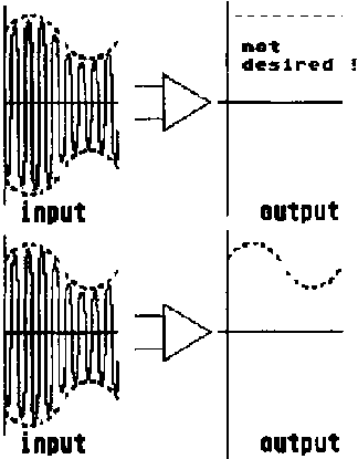
fig. 181
Obviously the proposed solution is not enough yet satisfying. Beside rectification we have to make sure that the AF-signal will decrease again, if the IF-signal peaks decreases again. The desired relation between in- and output-signal is shown in fig. 181 (lower part).
This can be achieved by a resistor connected in parallel to the smoothing capacitor as shown in fig. 184.
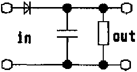
fig. 184
3. ADVANCED DETECTOR CIRCUIT.
In the above introduced detector circuit it will be made sure that the capacitor is selected as small as possible in order not to interfere to the AF-signal.
But in reality this method will cause always still a RIPPLE on top of the AF-signal as represented in fig. 185
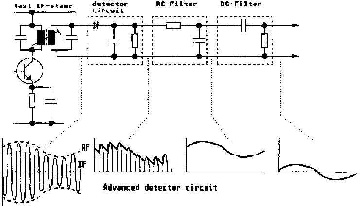
fig. 185
So always with this type of detector circuit the output will be a mixture of AF- and IF-signals.
In order to get only the AF-component of the input signal we find additional circuits necessary.
These additional circuits are the
RF-filter which removes the ripples.
DC-filter which removes the dc-component from the output of the RF-filter.
4. DIFFERENT KINDS OF DETECTOR CIRCUITS
A) Diode in series with R:
This is the type developed in the chapter before. It is the most often used one. It is loading the input-circuit which is normally a tuned circuit. In order to prevent that tuned circuit from distuning, the input signal is fed in via tapping transformer as shown in fig. 185.
B) Diode in parallel with R:
The advantage of this circuit is, that it is decoupled from the tuned circuit. Therefore we can connect this detector to any other potential.

fig. 186
Its disadvantage is: the resonant circuit is loaded even more than with the type shown above, because the resistor is always passed by a current while in the circuit above it is cutting off during one halfwave.
C) Demodulation by a voltage doubler
In order to produce a higher output voltage which will be less destorted, there is sometimes used a special circuit which is also used for special cases of rectification in order to reach higher output values. During the first halfwave with a positive potential at point A a diode 1 will be biased forward and C1 is charged. After this halfwave is over there will be found a certain voltage at C1 which is equal to the peak voltage of the first halfwave.
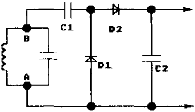
fig. 187
During the second halfwave diode 1 will be connected in reverse direction, but diode 2 will be biased in forward direction. And now capacitor C2 will be charged by the voltage originated from the tuned circuit and the voltage of C1.
At the end of this second halfwave C2 will be charged with a voltage two times as high as the peak voltage of the tuned circuit.
|
| ||||||||||||||||||||||||||||||||||||||||||||||||||||||||||||||||||||||||||||||||||||||||||||||||||||||||||||||||||||||||||||||||||||||||||||||||||||||||||||||||||||||||||||||||||||||
15. AGC-AUTOMATIC GAIN CONTROL
1. Purpose
This is the time when we can easily understand a special circuit which was not mentioned up to here. Its purpose is to cancel effects of the environment of a radio-receiver which can cause very intensive changes in reception of the wanted signal. Such a change of reception would cause a very strong change of the output-signal which means: a considerable change of sound volume. If there is not done anything about it, the receiver gives a reasonable sound at one moment a moment later the sound can be very weak or get unacceptable loud as a consequence of change of reception.
2. Function of the AGC-circuit
In order to stabilize the output signal we need an electric signal which presents the strength of the reception in order to use it for an automatical stabilization of the output-signal. The needed signal can be derived from the detector input signal. If we have a closer look to that signal we find, that this input signal has two components:
- the first part is the AF-component which normally does not change its amplitude during changes of reception strength.- the second part is the dc-component - the distance of the AF-sinewave from the noughtline. This second part is the one which gives us an information about the reception strength (as represented in fig. 188).
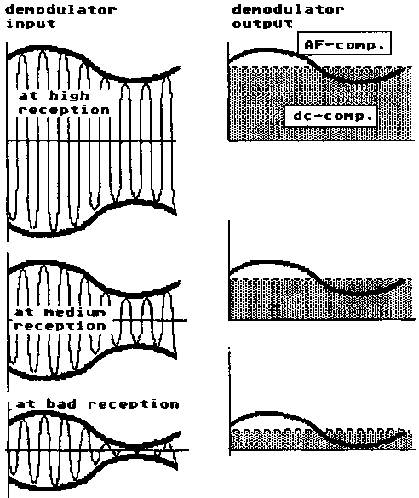
fig. 188
The wanted dc-signal can be produced by means of an RC-combination across the volume-control-potentiometer.
The voltage desired can be measured across the capacitor of that RC-combination, it is called Automatic-Gain-Control-voltage (AGC). It will be fed back to the biasing of the first IF-stage. If the AGC-voltage is growing it will decrease the amplification in that 1. IF-stage.
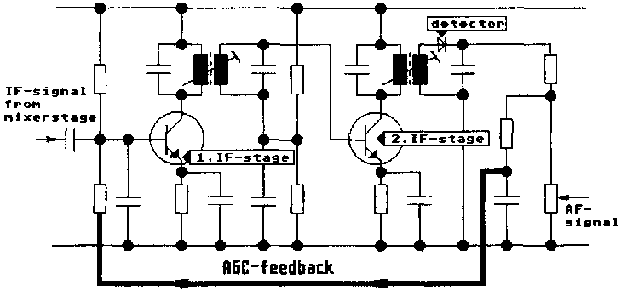
fig.
189
|
| ||||||||||||||||||||||||||||||||||||||||||||||||||||||||||||||||||||||||||||||||||||||||||||||||||||||||||||||||||||||||||||||||||||||||||||||||||||||||||||||||||||||||||||||||||||||
16. IF-AMPLIFIERS
Tuned amplifiers are Class-A-amplifiers with a parallel-type-tuned-circuit as collector-resistor.
The parallel-tuned-circuit has a characteristics as shown in fig. 191. Its impedance is maximum at the resonant frequency.
As bigger the collector resistance is as bigger is the amplification of such a class-A-amplifier.
This is the reason why this amplifier amplifies best the resonant frequency.
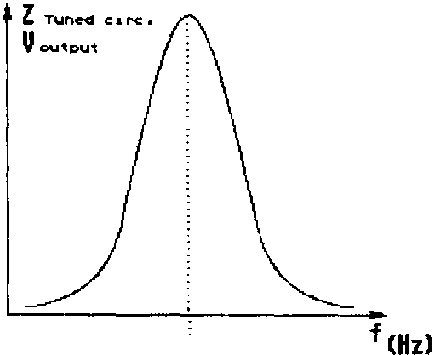
fig. 191
It is used most often for two purposes:
- Radio frequency amplifiers
- Intermediate frequency amplifiers
Its special advantages are:
1. The output signal of the mixer-stage has to be amplified anyway, but the IF-filter makes it possible for the IF-amplifiers to amplify only signals with a frequency very near around the IF-frequencies. Therefore the selectivity of those amplifiers can be adjusted to very high degrees.2. The IF-frequency is lower than the RF-and therefore we can easily avoid here problems which occur always at class-A-amplifiers with higher frequencies.
3. This kind of amplifier makes it especially simple to couple the next stage of the IF-amplifier exactly matching, because it is easy to provide the tuned circuit coil with a secondary coil which acts like a secondary coil in a transformer.
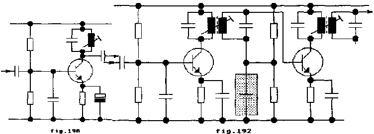
fig. 190, 192
SPECIALITIES IN IF-AMPLIFIERS
There are sometimes found some specialities with IF-amplifiers which should be mentioned and explained here.
- The capacitor found in fig. 192 parallel to the lower biasing resistor is introduced to the circuit in order to minimize the voltage-drop for the IF-signal via the loop: secondary coil of the tuned circuit (signal-source) base-emitter-junction and emitter-resistor-capacitor combination.- There are sometimes found IF-amplifiers coupled by a second tuned circuit formed by the secondary coil of the first filter coil and an additional capacitor (as also shown in fig. 192). In this case the response of the two stages (here mainly the bandwidth which is amplified) can be adjusted by the tiny iron core between both coils.
- Anyway the tuned circuits of IF-amplifiers have to be adjusted so that they amplify with a maximum at IF-frequency. But don't try this alignment deliberately - the adjustment of a new radio is undertaken in the factory with very high quality equipment which you will not have for your “alignment”.
- Sometimes you find a special connection within these amplifiers:
An RC-series circuit connected from the base of the transistor to the output side of the amplifier.This circuit is called a NEUTRALIZING CIRCUITS. It is necessary because there is always same capacitance between base and collector of the transistor. This capacitance will cause some feedback at higher frequencies which can cause very ugly oscillations of the amplification.
The neutralizing circuit cancels this effect.
fig. 193
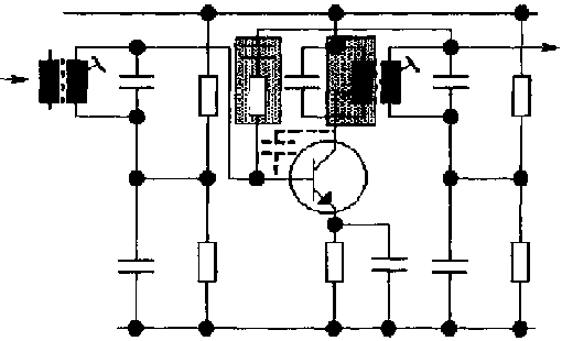
CHECK YOURSELF:
1. RF- and IF-amplifiers both work on radiofrequency range. Explain the main difference between them.2. Which kind of coupling is preferred between IF-amplifierstages, and why?
3. Why is the amplification of a tuned amplifier maximum just at a special frequency?
4. Under which condition would you try to realign an IF-frequency filter?
|
| ||||||||||||||||||||||||||||||||||||||||||||||||||||||||||||||||||||||||||||||||||||||||||||||||||||||||||||||||||||||||||||||||||||||||||||||||||||||||||||||||||||||||||||||||||||||
17. FEEDBACK
GENERALLY feedback is a process used in amplifier technology to feed a portion of the output signal back to the input.
Kinds of feedback:
In principle there are two possibilities of feeding back.
1. to add the output portion to the input signal.This is called POSITIVE FEEDBACK.
This kind of feedback always produces increasing changes, because any change of the input signal is amplified and a part of the output signal is fed back to the input signal.
Sooner or later the upper or lower border of amplification will be reached which means a sudden change of the output signal again and this means - the process starts again in opposite direction. Consequence: OSCILLATIONS.
2. to subtract the output portion from the input signal.
This is called NEGATIVE FEEDBACK.
This type of feeding back obviously reduces the amplification. This fact sounds at first as if it is a big disadvantage (for example it can cause the necessity of another amplifier stage).
But on the other hand it increases the STABILITY OF AMPLIFICATION and it decreases distortion. One possibility to produce negative feedback is already explained in chapter 12.4. It is the emitter-resistor in a class A amplifier which reduces the amplification but stabilizes its function.
Beside the already mentioned advantages we find with negative feedback an INCREASE OF INPUT IMPEDANCE OF AMPLIFIERS. A fact which is very important in connection with the problem of MATCHING.
The effects of feedback will depend very strong on the method of connection whether it is a series or a parallel connection. The parallel method of connection is not used in radio receivers. The methods of application of negative feedback are illustrated in the following diagrams:
VOLTAGE-SERIES FEEDBACK
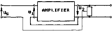
fig. 194
Results:
- reduction of gain and of distortion
- increase of input impedance
- decrease of output impedance
- improved frequency response
- stabilized gain
CURRENT-SERIES FEEDBACK
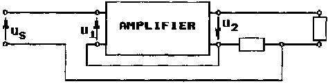
fig. 195
Actually current feedback is reading back a voltage which is depending on the current flowing in the output circuit.
Results:
- reduction of gain
- reduction of distortion
- improved frequency response
- increase of input impedance
|
| ||||||||||||||||||||||||||||||||||||||||||||||||||||||||||||||||||||||||||||||||||||||||||||||||||||||||||||||||||||||||||||||||||||||||||||||||||||||||||||||||||||||||||||||||||||||
18. OSCILLATORS
In a superhetreceiver the oscillator (often called the LOCAL OSCILLATOR) has to produce a high frequency which is:
fosc = freceived +fintern.frequ.
Therefore the oscillator must be able
- to produce a an RP-signal of a special and constant frequency and a constant amplitude.
- it must be easily possible to adjust its frequency.
HOW TO PRODUCE AN AC-VOLTAGE?
We know at the output of an amplifier the output voltage is dropping if the input voltage is increased. As explained in chapter 17 positive feedback causes oscillations. Therefore we have to find a solution how to get the output signal changing its phase for 180 degrees.
A solution is a circuit as shown in fig. 196 where we find a transformer used as collector resistor in a class A amplifier. If there is produced any change of the output signal in that circuit (for example by switching it on) there will be produced a voltage in the secondary coil of the transformer and this will cause an input signal which will be amplified and fed back again to the input...... and so on. The stage will carry on to produce oscillations.
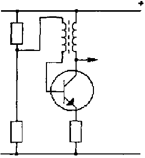
fig. 196
But this circuit cannot serve us as an oscillator for our local oscillator, because the frequency produced is not totally at random.
PRODUCTION OF A DEFINED FREQUENCY
If the primary coil is made part of a resonant circuit the highest current in this circuit can flow at resonant frequency. The highest current will cause the highest output signal at the secondary coil and this again will cause an oscillation with the resonant frequency of the tuned circuit. A circuit working on this principle is shown in fig. 197.
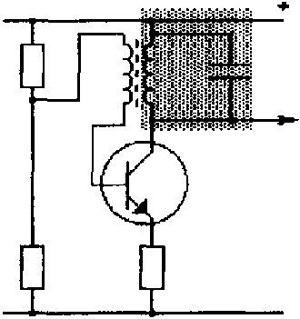
fig. 197
DIFFERENT KINDS OF OSCILLATORS.
Due to different problems when constructing an oscillator circuit there have been invented several oscillator circuits. But all of them are working on the general principle of positive feedback as derived above.
HARTLEY OSCILLATOR
To avoid the use of a transformer this circuit uses a portion of the inductor to produce the positive feedback.
COLPITT OSCILLATOR (fig. 198)
Here the feedback is coupled in at the emitter-resistor. The main advantage of that circuit is, that the base is connected via a capacitor to ground, which protects the circuit against interference from outside.
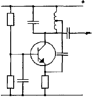
fig. 198a
ECO-CIRCUIT (fig. 198)
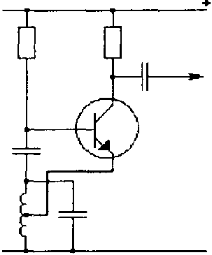
fig. 198b
Is made up in a so called common-collector-configuration. The main advantage of this circuit is, that the load current is flowing mainly over the collector-resistor.
The PUSH-PULL-OSCILLATOR which is actually a simple multivibrator circuit (used in a lot of other fields as well) The big advantage of this circuit is that the output can be matched exactly to the input by the secondary coil of the transformer.
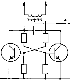
fig. 199
CHECK YOURSELF:
1. What is an oscillator necessary for in a superhet receiver?
2. How can oscillations be produced generally?
3. How can the frequency be kept stabil?
4. Describe at least two different kinds of oscillators!
|
| ||||||||||||||||||||||||||||||||||||||||||||||||||||||||||||||||||||||||||||||||||||||||||||||||||||||||||||||||||||||||||||||||||||||||||||||||||||||||||||||||||||||||||||||||||||||
19. FREQUENCY CHANGERS MIXERSTAGE
PURPOSE:
to change the incoming radio frequency to the selected intermediate-frequency (IF) by mixing the radiofrequency with the signal of the local oscillator.
GENERAL FUNCTION:
the mixerstage is mainly depending on two preconditions
a) the signals have to be added,
b) and the sum of the signals has to be amplified in a nonlinear way.
Adding of two signals can be achieved for example by connecting the output-coil of the oscillator and the secondary coil of the tuned circuit in series.
The signal at the output will look like fig. 200. As it is easy to see, there is not yet produced an evident signal which has the actual frequency of the IF.
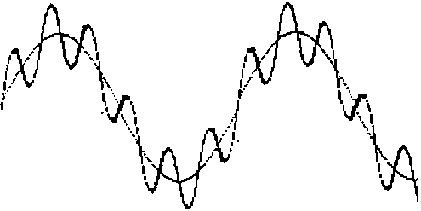
fig. 200
The IF-signal is produced by feeding the summarized signal into a so called nonlinear amplifier.
This is an amplifier similar like a Class A amplifier but with an extremly low biasing voltage. In fig. 201 is demonstrated how the signal is changed step by step. In order to get at last a signal modulated by the IF-frequency it will pass at last a transformer, which lets pass only the ac-component of the signal produced at point A of the stage. A practical circuit found
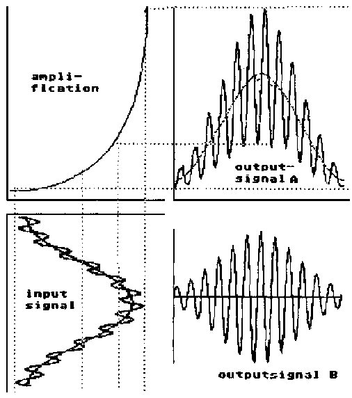
fig. 201
The two signals which have to be mixed together are injected via two channels. The RF-signal is injected as normal to the base of the transistor.
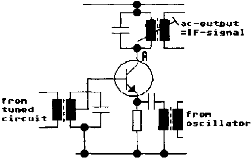
fig. 202
The signal of the local oscillator is injected at the emitter of the transistor.
COMMON MIXERSTAGE
Most domestic radio receivers use what is known as a “self-oscillating-mixer-stage”. In such a circuit the oscillater and the mixer function are achieved by a single transistor like shown in fig. 203.
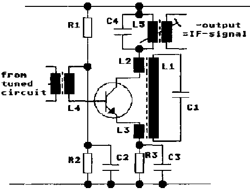
fig. 203
The oscillator-tuned-circuit is represented by L1 and C1. The feedback of the collector is injected via L2 and the oscillator-output is coupled to L3 at the emitter to be mixed together with the RF-from the tuned circuit coming from L4 connected to the base of the transistor. A small starting bias for the oscillator is provided by R1 and R2 and a reverse bias is R3 and C3.
The circuit selects via C4 and LS the intermediate frequency which is produced via the mixing process as well and feeds the IF via the tuned circuit L5 and C4 to the next amplifier stage.
CHECK YOURSELF:
1. What is HETERODYINING? What is its advantage?2. What is a mixerstage necessary for in a superhet receiver?
3. Mention the type of radio receiver which has a frequency changer!
4. What happens during the process of hereodyning? What is the output of a frequency changer?
5. Which preconditions are necessary to mix two frequencies properly?
|
| ||||||||||||||||||||||||||||||||||||||||||||||||||||||||||||||||||||||||||||||||||||||||||||||||||||||||||||||||||||||||||||||||||||||||||||||||||||||||||||||||||||||||||||||||||||||
20. DECOUPLING CIRCUITS
GENERALLY:
If you recollect the circuit of a simple Class A amplifier you can yourself very easily predict what would happen in this circuit if there is any change of supply voltage.
A change of supply voltage - even if it is very tiny - will cause a change at the centrepoint of the base-voltage divider. This causes a change of the base-emitter voltage at the transistor and this will cause an output signal.
As long as we observe only a single amplifierstage, we will not see a big problem connected with this effect because we use anyway a rather steady supply voltage and therefore we must not expect too strong changes of its values. But if the amplifier observed is an early stage of a radio receiver, followed by several amplifier stages, we will face much bigger problem because of two reasons:
1. the signal caused by the voltage changes before was very tiny but now it is amplified vey the next amplifierstages for up to several tenthousend times. This means: at the output of the receiver we will have considerable signal now.2. Such a signal causes at the power amplifier a considerable big change of load current and this will cause - even at a stabilized power supply - at least a tiny voltage drop .... just the voltage drop which was the beginning of our consideration.
The effect which we derived here is a so called POSITIVE FEEDBACK and this causes always OSCILLATIONS - “MOTORBOATING” as the “Fundis” call it.
fig. 204
This is the reason why almost always all the stages except the power amplifier are DECOUPLED.
Sometimes some stages together sometimes each stage separately. Decoupling is achieved by nothing else than an ac-filter made up from an RC-series connection.
fig.
205
|
| ||||||||||||||||||||||||||||||||||||||||||||||||||||||||||||||||||||||||||||||||||||||||||||||||||||||||||||||||||||||||||||||||||||||||||||||||||||||||||||||||||||||||||||||||||||||
21. MATCHING OF AMPLIFIERSTAGES
A single amplifierstage is only able to amplify within certain limits. If these limits are not observed thoroughly there will arise heavy distortions.
In most electronic devices the overall-amplification (amplification of the whole device) is far beyond the limits of a single stage. Therefore it is necessary to “couple” amplifierstages together.
If we amplify a signal via several stages the connection of such stages looks like a chain of circuits as shown in fig. 209.
fig. 209
Each part of that chain consists of an
- “output-side” (which plays a part like an energy source here) and an
- “input-side” (which stands here for the consumer of the energy delivered by the output).
The aim is to produce at last a signal of a satisfying power as necessary and a shape as similar in shape as possible to the input signal of that chain.
The output power of an amplifierstage is depending on:
- the amplification factor of the stage, and
- the input-power of the signal.
So the amplification-factor for one is given for a certain stage, the factor which has to be kept in mind during coupling two stages, is to make sure to get as much as possible energy from the output of stage “n” to the input of stage “n+1”. The method of achieving this is called MATCHING.
It is done on the basis of the following thoughts:
If you consider an amplifier as a “black box” you can easily see that the input draws a certain current at a certain voltage (so consuming a certain power).
All in all the input behaves like a resistor. As we talk about ac-voltage and currents we call it an impedance. Therefore we call this behaviour of the amplifier its: INPUT-IMPEDANCE
fig. 210a
The energy consumed by the input impedance is delivered by the output of the last stage. So the output acts here like a voltage-source. But as we know, each voltage-source has its internal resistance. Again we should keep in mind, that we deal with ac-values and therefore we call this internal resistance of the output the: OUTPUT IMPEDANCE.
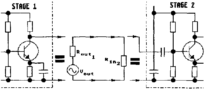
figure
As we learnt earlier:
A voltage source is transmitting its maximum of power to a consumer if the load resistor is equal to the internal resistor of the source as it is explained once more in fig. 212.
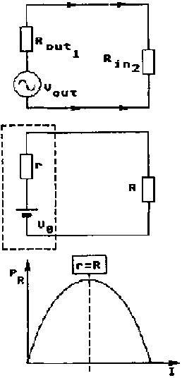
fig. 212
We can use this knowledge accordingly to our matching problem and therefore we can state:
AMPLIFIERS ARE MATCHED EXACTLY IF THE OUTPUT - IMPEDANCE OF THE LAST STAGE IS EQUAL TO THE INPUT-IMPEDANCE OF THE FOLLOWING STAGE.
There are several possibilities to calculate the input- and output-impedance theoretically. But these methods would be beyond the limits of this course. Here we will mention only a possibility to measure the impedances.
If a radiotechnician intends to couple amplifiers together which have not been coupled before, he has to know how to measure these two values.
MEASUREMENT OF THE INPUT-IMPEDANCE
As Ohm's Law shows, the input resistance can be determined by measuring the input voltage and the input-current. But especially to measure the current is very difficult. So another method has been introduced:
A signalgenerator with a preferable low output-impedance is needed. Most of the signalgenerators are stabilized ones nowadays and therefore we can expect the output-impedance to be almost cero.
At first we set the signalgenerator to a voltage reasonable for the amplifier which should be researched.
The amplifier is connected to the signal-generator via a potentiometer whereby the potentiometer should be set to the highest values possible as shown in fig. 213.

fig. 213
Now the potentiometer is slowly set to lower resistances, whereby we observe the voltage measured at the input terminals of the amplifier.
As you might have concluded already:
THE INPUT IMPEDANCE OF THE AMPLIFIERSTAGE IS EQUAL TO THE RESISTANCE OF THE POTENTIOMETER WHEN THE INPUT-VOLTAGE HAS REACHED EXACTLY HALF OF THE ORIGINAL VALUE (Before reducing the resistance).
MEASUREMENT OF THE OUTPUT-IMPEDANCE
The output resistance is - as explained above - like the internal resistance of the voltage-source which the amplifier-output represents. In order to determine it, we have to measure the voltage-drop at the output terminals caused by a current increase. But again it would be too difficult to measure the current. Therefore we use again another method. The output-voltage is measured at first without any load. Now we connect a potentiometer to the output of the amplifier whereby we set first the potentiometer to the highest resistance. Then we start to decrease slowly the resistance whereby we observe the voltmeter.
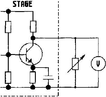
fig. 214
As you might have concluded already:
THE OUTPUT RESISTANCE OF THE AMPLIFIERSTAGE IS EQUAL TO THE RESISTANCE WHICH THE POTENTIOMETER IS SET TO WHEN THE OUTPUT-VOLTAGE HAS REACHED EXACTLY HALF OF THE ORIGINAL OUTPUT VOLTAGE.
EXCEPTION: Very often it is not practicable to decrease the output voltage to 50%. In this case there might occur a heavy distortion. So it is often better to reduce the output voltage only to 90% of the original value. The output resistance is then 1/9 times as high as the resistance to which the potentiometer is set too.
|
| ||||||||||||||||||||||||||||||||||||||||||||||||||||||||||||||||||||||||||||||||||||||||||||||||||||||||||||||||||||||||||||||||||||||||||||||||||||||||||||||||||||||||||||||||||||||
22. COUPLING OF AMPLIFIERSTAGES
GENERAL REMARK
Amplifierstages have a HIGH INPUT IMPEDANCE while they have on the other hand A RATHER LOW OUTPUT IMPEDANCE. As explained during the chapter MATCHING this causes problems if we want to secure an efficient coupling.
COUPLING BY TRANSFORMERS
The most effective way to couple two amplifier stages for ac-signals is to couple them by a transformer.
In this case it is easily possible to use as a collector resistance of the first amplifier-stage which will deliver the signal the primary coil of the transformer. The secondary coil of the transformer is connected within the path from the biasing circuit to the base of the second.
An example is shown in fig. 206. By choosing the fitting number of turns it is possible to adjust the impedances of the two coils exactly to their complimentary impedances within the amplifierstages.
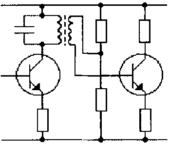
fig. 206
This method was used especially in the early days of transistor technology, when it was necessary to have as few transistors as possible (because of their high prices at that time).
Now you know all the different blocks of a simple AM-radio and you should be able to read the circuit diagram below.
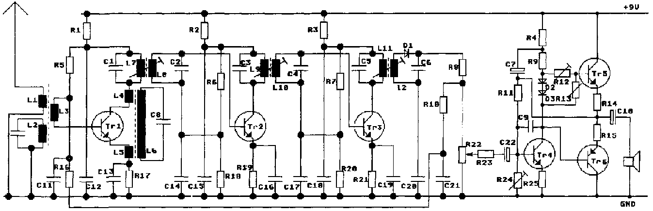
figure
CHECK YOURSELF:
1. What does FEEDBACK mean?
2. What advantage has:
a) positive feedback
b) negative feedback?
3. What does “matching” mean?
4. Which type of coupling of amplifier-stages is the most accurate one?
5. Can you differentiate the blocks of the radio?
6. Explain what the components in the blocks are for!
|
| |||||||||||||||||||||||||||||||||||
Radio and Electronics (DED Philippinen, 66 p.)
23. RADIO SERVICING
23.1. IMPORTANCE AND SUBJECT OF FAULT FINDING
Repair of a radio is an economical activity (if done professionally). Therefore it is an activity during which somebody who is undertaking it has to keep in mind economical questions in order to be able to earn his living.
Therefore the question - which method of fault finding should be chosen in a special case - will be answered normally under its economical aspect.
During the overall activity of repairing a radio the section FAULT FINDING has an overwhelming importance. If a fault has been located it has lost its “horror”, because its remedy requires only some rather simple skills and some knowledge about components and materials.
If repair is done as a business, fault finding is a main factor of calculation of costs. The time consumed for it is a very big portion of the overall time spend for the repair. A quick location of faults is therefore reducing the costs and gives so the professionalist a big advantage in competition.
To be able to choose the fitting method of fault finding under special circumstances, it is necessary to have a general viey of all possible methods to track down faults. An important role play the measuring instruments.
Instruments, finding devices, signalgenerators and so on, are items which are very expensive and therefore must enter the calculation of costs as well.
Even if a beginner does not have all instruments available on the market he has a big advantage if he has a profound knowledge of all possible methods because he is only then able to apply the best method which will cause the smallest costs.
23.2. FAULTS AND FAULT FINDING
Repair of devices working on high frequencies is one of the most difficult problems which modern technology can force us to solve.
Almost every radioreceiver consists of a big number of components which seem on the first glance all OK.
Each of them could be the cause of the fault. They do not necessarily look different if they are in a condition of proper working or if they are really faulty.
With our normal senses we can recognize only very minor differences if at all. Burnt resistors, open circuits, spilt condensers, burnt coils and so on, are rather rarely to be found.
In most cases we can only observe effects of faults of which the fact that the loudspeaker is totally dead could be simplest one. Since during fault finding we cannot achieve any development by using our senses, measuring instruments must be applied in order to display the electrical condition in and around the components.
Only this enables us to draw conclusions. The stringing up of such conclusions is defining the method which has to observe all conditions which are important for the operation of the whole device.
THEORETICAL KNOWLEDGE IS ESSENTIAL
If fault finding is not to be done at random, theory is a must. Nobody is able to repair a device reasonably if he does not understand the function of each component and each block of components.
At this point we find the big difference between all other kind of electrical equipment and especially high-frequency equipment. Somebody can be a rather good mechanical engineer (or “fundi”) and for example repair a typewriter very well without knowing the laws governing leverage. Without knowing the laws and effects of electricity, of dc-currents, ac-currents, high- and low-frequencies and so on, nobody will be able to repair an electrical device especially not a radio.
If somebody is starting to repair such a device his first thought has to be to follow the idea which has been put into action with that device.
Looking to the big number and the different kinds of components. It is mostly possible to guess at least which kind of receiver is brought to you.
It would be possible to trace all the circuits contained in it, but this would be very tiresome and a very long procedure. It is obviously much better to collect a good number of circuit diagrams and to refer to the fitting one immediatedly.
But even if the fitting circuitdiagram is available it makes no sense if this is only a collection of symbols and values for the repairing person. He must be able to draw conclusions about the function of each component and he must be able to predict the function of each block within the whole arrangement.
Theoretical reflections must accompany the repair from start to the end.
OBSERVATIONS OF THE RADIO OWNER
Not at all each fault in a radio can be observed if you only operate it only for some minutes. And not at all the radio must be totally dead if it is faulty.
Moreover there are a lot of possible defects which can cause a radio not to operate properly but to operate anyhow. Especially in cases of these defects “in between” (totally dead or normal function) the owner and user of the radio can give us some helpful hints for the repair if we ask him in a clever manner.
It is an additional skill of a radio repair professionalist to talk with his costumers in a way which will enable him to get a good clue for his work. But he has to keep in mind: the costumer is a layman whose conclusions are very often wrong. His sorrow that the bill could be too high may lead him to “bend” the truth.
It is the skill of a professionalist to reach as nears possible to the truth. For example to find out if a fault occured all of a sudden or if there were observed some small defects already before. It is also possible to find out if something has been burning at the fault. You should not neglect this simple method of investigation with the costumer. It can help you to save time with some preliminary steps in fault finding and it will help the costumer to develop a trustful relation to the repairing person, a condition will pay off very soon in getting more costumers.
Every radio technician should act somehow like a good medical doctor.
STATISTICS OF FAULTS
As more experienced a radio technician is, as more he tends to do some preliminary checks before he starts the actual systematical fault finding. That is because experience taught him that there are a certain number of faults which appear much more often than others. Moreover there are certain blocks of radios which show-more often faults than others. If one takes this different probability of faults in account he can draw conclusions where the fault might be located most probably. These experiences can of course influence the method of fault finding. For this reason there was undertaken for quite a number of years a research concerning all kinds of radio receivers. After introduction of integrated circuits there was done a second research of the “fault behaviour” of this new type of receivers.
The results of these two researches are displayed in fig. 217.
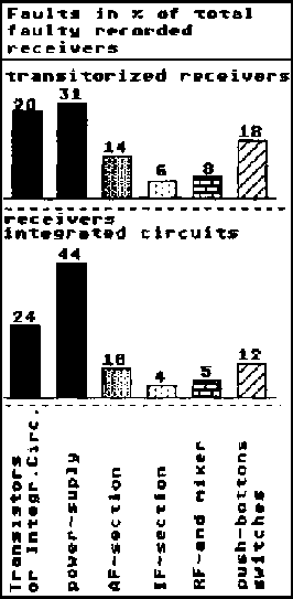
fig. 217
The overall number of receivers with integrated circuits having been faulty was remarkably less than the number of only transistorized receivers.
It is nor yet clear if this was due to the fact that integrated circuits equipped receivers have been fairly new in service while normal transistor receivers had already a rather long service time.
In both statistics it is obvious that most of the faults occure in the powersupply section of radios.
Mechanically originated faults like they are caused very often in the push-bot-ton-gear for changing bands or stations are also rather often found. While the faults in HF- and IF-blocks are found very seldom.
Interesting is too, that the number of faults in the AF-sections of radios which integrated circuits is remarkably lower than in radios equipped with normal transistorized circuits.
From these statistics you can draw the following CONCLUSION:
IF YOUR HAVE NO IDEA WHERE TO START WITH FAULT FINDING IT IS MOST PROMISING TO START TO CHECK FIRST THE POWER SUPPLY AND THEN THE AF-SECTION.
THE PRE-CHECK
If you have no clue at all where to start which fault finding you should undertake some simple checks first of all. Aim of this PRE-CHECK is to find out simple faults before you start the actually time consuming fault finding procedure:
1. Switch on the radio, turn the volume control to full. Now check if you hear some noise at the instant of switching. If not: CHECK THE POWER-SUPPLY!2. While you do the first step (described above) it is adviceable to check by touching the power-transistors, or the power amplifier IC if it is getting hot. If this happens SWITCH OFF IMMEDIATEDLY - THERE MUST BE A SHORT CIRCUIT WITHIN THE POWER-AMPLIFIER.
3. Now you should have a close look to the circuit boards. You should look for any components which show destruction (burnt resistors, spilt capacitors, loose wires or interrupted conducting paths on the printed circuit).
4. Now touch the antenna socket with the antenna plug. You should hear some noise - if not - YOU CAN BE SURE, THAT THERE IS NO OR NOT ENOUGH AMPLIFICATION OF THE INPUT SIGNAL. To localize this fault,....
5. ... Switch the receiver to “sound channel” and touch the audio input with your finger.
You should hear some noise now.
if this is the case:
CONCENTRATE ON IF-STAGES AND MIXERSTAGES
if this is not the case:
CONCENTRATE ON THE AF-AMPLIFIERS.
After this PRE CHECK you can start with the systematical fault finding as it will described now.
23.3. FAULT FINDING METHODS
Repair is mainly ... “setting the device back to the condition of normal operation, because we presume the device brought to us for repair has worked before properly”. We can presume as well most of the preconditions - necessary for correct operation - are still given. Only a few - if not a single - components are defect. Such a defect causes:
- a lag of voltage at a number of terminals
- lag of current through some wires-
- change of resistance of the component.
Measurement of voltage, current or resistance can therefore serve as a reference to locate the actual fault. When you are searching for those effects of faults the various measured values are compared with the values expected (or given in the data sheet).
We call the methods:
VOLTAGEANALYSING
CURRENTANALYSING and
RESISTANCEANALYSING.
The voltageanalysing is the most often used one, because it can be carried out without any mechanical change of the device (voltage can be measured in parallel)
VOLTAGEANALYSING
Here we mostly start to measure the voltages at the power-supply and then the voltages at the supplying terminals of the blocks.
If we find a voltage missing or a strange value we have to consider what could be the reason for this effect.
WHICH MEASURING INSTRUMENTS SHOULD BE USED FOR VOLTAGEANALYSING?
In practice the measuring instrument necessary for fault finding plays an important role.
Very often it determines the measurements which can be undertaken, because it will determine the misreading in a certain case.
The most often used instrument in radio servicing was the moving coil instrument with an internal resistance of at least 50 kOhms.
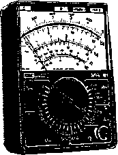
figure
If anyhow possible, it should have a protection against overload and and it should be mechanically strong in order to be able it with you for outdoor repairs.
A disadvantage of these moving-coil instruments is the sometimes rather low internal resistance especially within the low voltage ranges (below 1 V).
For more complicated and sophisticated measurements there are available VALVE-VOLTMETERS or TRANSISTORIZED VOLTMETERS.
These are measuring instruments which are fed by a dc-amplifier of a very high input impedance and a output impedance matched to a moving coil instrument. Another type of instruments which is available since a few years are the so called DIGITAL-VOLTMETERS, which have dc-amplifier and an electronic circuit which shows the value of the voltage as a sequence of figures. The advantage of this type in comparison with other types is, they are easier to read small differences in values, but it is a problem to read it if the values are continuing to change.
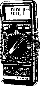
figure
CURRENT ANALYSING
Real current measuring is undertaken only in very special cases, because it is necessary to open the circuit, and this means actually to dissolder a terminal of a component. This is time consuming and endangering the circuit, because you could break a connection.
Therefore direct current analysing is used only in a few special cases:
- if it is urgently necessary (because voltage measurement does not help anymore)- or if it is extremly simple to undertake it (for example at a fuse, a contact of a switch or special plugged in links).
But you can very often measure the current INDIRECTLY by measuring the voltage across a resistor which is passed by this current. If you know what is the resistance of this resistor you can determine the current by Ohm's Law.
TOTAL CURRENT MEASUREMENT
By measuring the total current of a receiver it is also possible to draw some conclusions especially about the condition of the power-amplifier.
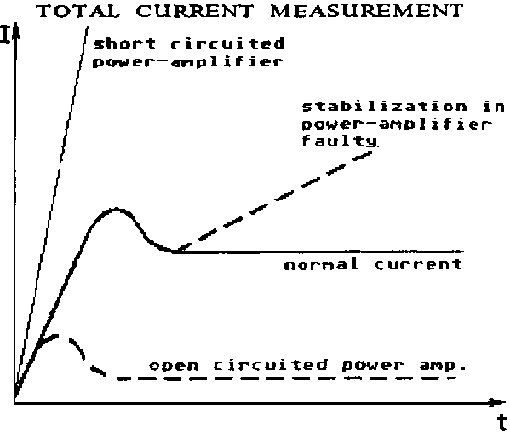
fig. 219
Fig. 219. shows how the current behaves in different cases.
But keep in mind to do this measurement at least in the beginning with the instrument set to the biggest current measuring range available (as smaller the measuring range as bigger the internal resistance and therefore the influence of the measuring instrument).
STATIC CURRENT MEASUREMENT
Another often used measuring method is to measure the current flowing in transistors of the power-amplifier while there is no sound produced.
Specially for this purpose we find very often links which can either be removed by hand or which can be easily dissoldered. If there is found a too high value it is very likely that one of the power-transistors is blown.
RESISTANCE ANALYSING
RESISTANCE ANALYSING HAS TO BE DONE WHILE THE DEVICE IS SWITCHED OFF ONLY (otherwise you can easily spoil the measuring instrument).
In case of valve radios it is possible to measure most of the resistances while everything is left like it was. In transistorradios, we must dissolder very often at least one terminal of the component whose resistor we are planning to measure.
SIGNALINJECTION AND SIGNALTRACING
All the fault finding methods described above are aiming at to find out if the normal operation conditions are given at a certain spot or not.
A very different approach is to undertake “spot-checks”.
This is done in order to find out:
- either up to which stage is the receiver still working properly.
- or from which stage on is the receiver still working.
The first method is done by injecting a signal at the input (aerial) and finding out from which stage to find out from which stage on the receiver is “dead” (signaltracing).
The second method is done by injecting a signal first very near to the output - for example at the input of the AF-stage - then a step backwards - for example at the input of the detector - and so on up to the aerial (signalinjecting). Of course this can only be carried out while the device is switched on and set to a reasonable volume.
It should be stressed that both of those methods will not allow to find out the faulty component but only the faulty block in the receiver. These methods are very fast. But if you want to apply them really professionally the equipment necessary is rather expensive.
THE FINGERTEST
ONLY ADVICEABLE IN TRANSISTORRADIOS!
The cheapest and easiest accessable “instrument” for signal injection is your finger. Your body is collecting electric and magnetic fields of your environment. These “signals” can be heard if you inject it to the AF-section of the radioreceiver. At a normal transistorradio we should hear a humming sound, if we touch for example the hot end of the volume control potentiometer. It is obvious, that this is very coarse and limitted method.
SIGNALINJECTORS
We know mainly three types of signalinjectors which can be used in radio servicing practice.
The cheapest possibility is a so called.
MULTIVIBRATOR.
This is an electric device which produces a flat-topped signal of any frequency. The trick - used here - is that easy flat-topped signal includes a wide frequency range of sinusoidal signals. So the multivibrator produces a “distortion” over the whole range of frequencies processed in a radio. Therefore we can inject its signal at every point of the receiver and it will have effect anyway. The problem with this kind of signalinjector is that we do not know which frequency is causing now the effect heard at the speaker.
If we want really to inject defined signals we have to use signal generators.
THE AUDIO FREQUENCY GENERATOR.
It has normally a frequency range of 10 Hz to 100 kHz. you can easily conclude, that you can use this generator only for the AF-stage and the demodulator.
THE RADIO FREQUENCY GENERATOR
If you want to inject defined signals to the IF-stages or to the aerial you need this type, which is normally able to produce frequencies between 100 kHz up to 300 MHz. It is equipped with a modulator section which can modulate the output-signal either with a fixed frequency (for example 1 kHz) or with an externyl produced audio signal.

figure
ANALYSING OF EFFECTS OF INJECTED SIGNALS
If we inject a signal we do it always by having a special effect in mind, which should be shown by the receivers output if the stage under research is in order. The term “shown” is already misleading, because without a measuring instrument we cannot see anything but only hear the effect.
Our ears are able to adapt to a very wide range of sound volume and therefore we ourselves are very poor “measuring instruments”.
In case of a fault for which we need a very exact reading of the output signal we need a reliable instrument for this signal.
We can either use a so-called DUMMY LOAD (a fitting reistor which represents the speaker for example) and a fitting moving coil instrument, or - much better - an OSCILLOSCOPE which is found more and more often in radio workshops nowadays. If we have access to a two channel oscilloscope we are extremly lucky because in this case we can measure input and output-signal at the same time, and we can compare it on the screen of the “scope”.
Then we can observe: - the frequencies - the shape - and the amplitudes of both signals. A situation which is “the dream” of a lot of radio technicians these days. For this reason here - at the end of this script - shall be given a short introduction to the use of an oscilloscope.
figure
|
| ||||||||||||||||||||||||||||||||||||||||||||||||||||||||||||||||||||||||||||||||||||||||||||||||||||||||||||||||||||||||||||||||||||||||||||||||||||||||||||||||||||||||||||||||||||||
24. THE USE OF THE OSCILLOSCOPE
Oscilloscopes range from simple general-purpose instruments to highly sophisticated pieces of equipment.
THE CATHODE RAY TUBE
Basically, however, any oscilloscope consists of a cathode ray tube with associated electronic circuitry which enables us not only to measure signal waveform's, amplitude, frequency etc. but also to see the actual waveform displayed on a screen enabling us to check the signal for distortion - an important factor in circuit repair and adjustment.
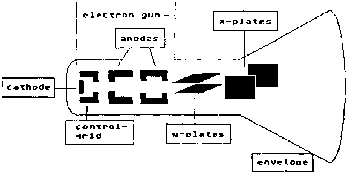
figure
Fig. 226 shows a simple schematic diagram of the heart of any oscilloscope: the cathode ray tube, which consists of an electron gun, envelope and screen.
The electron gun contains a cathode which, when heated, emits electrons. These electrons are attracted from the cathode by a cylindrical anode carrying a very high positive voltage. The electrons are then accelerated and move at high speed in direction of the screen.
In fig. 226 you see that, in practice, the cylindrical anode is in two parts, called focussing anode an accelerating anode. By adjusting the potential difference between the two anodes, the electron-flow is focussed to a small spot at the point where it reaches the screen. The screen is coated with fluorescent material. So that a bright spot shows the point of impact.
The brillance of the spot can be adjusted by means of a negatively biased control-grid placed between the cathode and the anode. If the control-grid is made more positive or negative, a correspondingly greater or smaller quantity of the electrons is attracted by the anode, thus varying the intensity of the spot on the screen.
Between the anode and the screen there are two sets of deflection plates set at right angles to each other: two parallel plates used for horizontal deflection of the spot - the so called X-plates, and two parallel plates for the vertical deflection of the spot - the so called Y-plates.
When a voltage is applied between the two X-plates, the electron beam will be deflected in horizontal direction and thus the spot on the screen will move horizontally. The amplitude of this deflection is a function of the amplitude of voltage applied to the plates and the direction of the deflection depends on the polarity. In the same way the Y-plates are used for the vertical deflection of the electron beam.
If a sine-wave voltage is applied to the Y-plates, the electron beam will be alternately attracted and repelled by the plates and the spot will move up and down the screen.
Due to the persistence of the fluorescent material on the screen face, a solid vertical trace line will appear whose length will depend on the magnitude of the sine-wave voltage. Similarly, if the same voltage is applied instead to the X-plates, a horizontal trace will appear.
FUNCTION OF THE “SCOPE”
In practice, the signal waveform to be studied is applied to the Y-plates, whilst the X-plates are employed to provide a variable, linear time-base by means of a sawtooth waveform generator (see fig. 227).
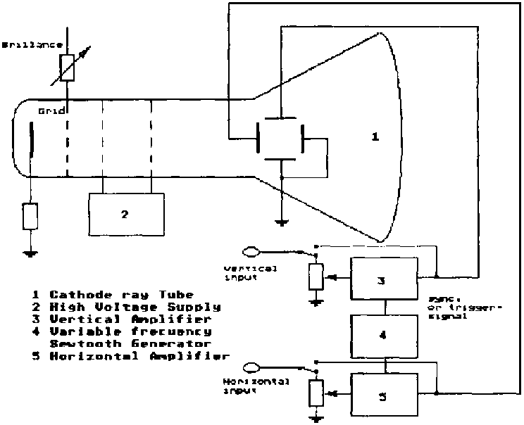
fig. 227
The voltage delivered by this generator increases linearly with time. Hence, the spot on the screen moves with constant speed from left to right and its position is a function of time. At the end of this deflection period, the voltage returns to its original value very quickly.
The frequency of the time-base voltage can be varied by means of a time-base or velocity control. When an ac-voltage is applied to the Y-plates, it then appears in its familiar sine-wave form on the screen of the cathode ray tupe through the combination of the waveforms acting on the electron beam.
Finally, as can be seen in fig. 227. amplifiers are connected to the deflection plates, so that small signals can be seen more clearly and measured more accurately. In most oscilloscopes the amplifiers can switched out for the measurement of large signals, which in themselves will give sufficiently large traces. It is of course important when a periodic signal is displayed on the screen that at the beginning of each period of the time-base the signal always starts at the same place of the screen. This can be done in two ways:
SYNCHRONISATION OR TRIGGERING.
A synchronisation circuit ensures that the frequency of the time-base (or a multiple of it) is exactly the same as the frequency of the signal.
The frequency of the time-base must, therefore, be manually adjusted until the signal on the screen does not move anymore.
A triggered time-base is started by the signal. This means that, after a given time, the time-base waits for the next positive or negative edge of the signal. This system is commonly used in modern oscilloscopes.